- 您现在的位置:买卖IC网 > PDF目录368232 > PSD835G2-12JI (意法半导体) Configurable Memory System on a Chip for 8-Bit Microcontrollers PDF资料下载
参数资料
| 型号: | PSD835G2-12JI |
| 厂商: | 意法半导体 |
| 英文描述: | Configurable Memory System on a Chip for 8-Bit Microcontrollers |
| 中文描述: | 在8片位微控制器可配置存储系统 |
| 文件页数: | 10/110页 |
| 文件大小: | 570K |
| 代理商: | PSD835G2-12JI |
第1页第2页第3页第4页第5页第6页第7页第8页第9页当前第10页第11页第12页第13页第14页第15页第16页第17页第18页第19页第20页第21页第22页第23页第24页第25页第26页第27页第28页第29页第30页第31页第32页第33页第34页第35页第36页第37页第38页第39页第40页第41页第42页第43页第44页第45页第46页第47页第48页第49页第50页第51页第52页第53页第54页第55页第56页第57页第58页第59页第60页第61页第62页第63页第64页第65页第66页第67页第68页第69页第70页第71页第72页第73页第74页第75页第76页第77页第78页第79页第80页第81页第82页第83页第84页第85页第86页第87页第88页第89页第90页第91页第92页第93页第94页第95页第96页第97页第98页第99页第100页第101页第102页第103页第104页第105页第106页第107页第108页第109页第110页
PSD835G2
PSD8XX Family
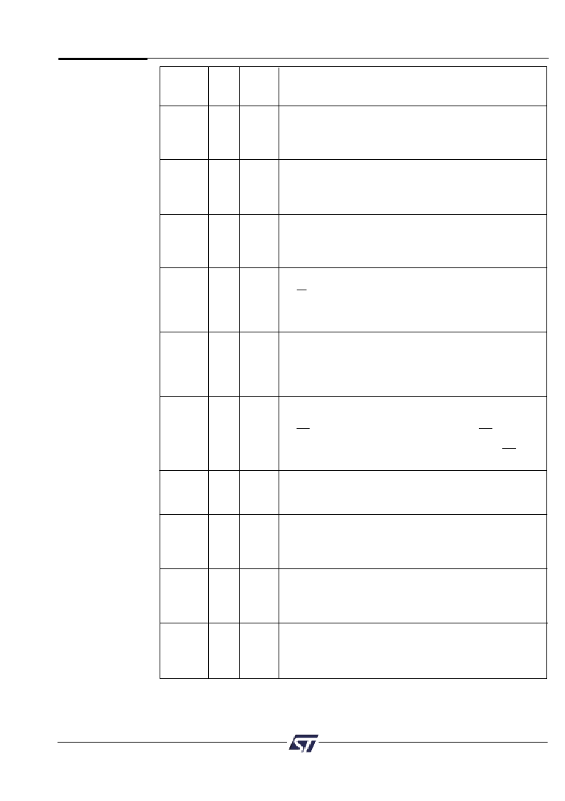
Pin*
(TQFP
Pin Name Pkg.)
PA0-PA7
Type
I/O
CMOS
or Open
Drain
Description
51-58
Port A, PA0-7. This port is pin configurable and has multiple
functions:
1. MCU I/O — standard output or input port
2. CPLD Micro
Cell (MCell A0-7) output.
3. Latched, transparent or registered PLD input.
Port B, PB0-7. This port is pin configurable and has multiple
functions:
1. MCU I/O — standard output or input port.
2. CPLD Micro
Cell (MCell B0-7) output.
3. Latched, transparent or registered PLD input.
Port C, PC0-7. This port is pin configurable and has multiple
functions:
1. MCU I/O — standard output or input port.
2. External chip select (ECS0-7) output.
3. Latched, transparent or registered PLD input.
Port D pin PD0 can be configured as:
1. ALE or AS input — latches addresses on ADIO0-15 pins
2. AS input — latches addresses on ADIO0-15 pins on the
rising edge.
3. Input to the PLD.
4. Transparent PLD input.
Port D pin PD1 can be configured as:
1. MCU I/O
2. Input to the PLD.
3. CLKIN clock input — clock input to the CPLD
Micro
Cells, the APD power down counter and CPLD
AND Array.
Port D pin PD2 can be configured as:
1. MCU I/O
2. Input to the PLD.
3. CSI input — chip select input. When low, the CSI enables
the internal PSD memories and I/O. When high, the
internal memories are disabled to conserve power. CSI
trailing edge can get the part out of power-down mode.
PB0-PB7
61-68
I/O
CMOS
or Open
Drain
PC0-PC7 41-48
I/O
CMOS
or Slew
Rate
PD0
79
I/O
CMOS
or Open
Drain
PD1
80
I/O
CMOS
or Open
Drain
PD2
1
I/O
CMOS
or Open
Drain
PD3
2
I/O
Port D pin PD3 can be configured as:
1. MCU I/O
2. Input to the PLD.
CMOS
or Open
Drain
I/O
CMOS
or Open
Drain
PE0
71
Port E, PE0. This port is pin configurable and has multiple
functions:
1. MCU I/O — standard output or input port.
2. Latched address output.
3. TMS input for JTAG/ISP interface.
Port E, PE1. This port is pin configurable and has multiple
functions:
1. MCU I/O — standard output or input port.
2. Latched address output.
3. TCK input for JTAG/ISP interface (Schmidt Trigger).
Port E, PE2. This port is pin configurable and has multiple
functions:
1. MCU I/O — standard output or input port.
2. Latched address output.
3. TDI input for JTAG/ISP interface.
PE1
72
I/O
CMOS
or Open
Drain
PE2
73
I/O
CMOS
or Open
Drain
Table 5.
PSD835G2
Pin
Descriptions
(cont.)
9
相关PDF资料 |
PDF描述 |
|---|---|
| PSD835G2-12M | Configurable Memory System on a Chip for 8-Bit Microcontrollers |
| PSD835F3V-12B81 | Configurable Memory System on a Chip for 8-Bit Microcontrollers |
| PSD835G2V-12B81 | Configurable Memory System on a Chip for 8-Bit Microcontrollers |
| PSD835F1-20U | Single Ended Active Clamp/Reset PWM 16-SOIC -40 to 85 |
| PSD835F1-20UI | Single Ended Active Clamp/Reset PWM 16-PDIP -40 to 85 |
相关代理商/技术参数 |
参数描述 |
|---|---|
| PSD835G2-70U | 功能描述:静态随机存取存储器 5.0V 4M 70ns RoHS:否 制造商:Cypress Semiconductor 存储容量:16 Mbit 组织:1 M x 16 访问时间:55 ns 电源电压-最大:3.6 V 电源电压-最小:2.2 V 最大工作电流:22 uA 最大工作温度:+ 85 C 最小工作温度:- 40 C 安装风格:SMD/SMT 封装 / 箱体:TSOP-48 封装:Tray |
| PSD835G2-90U | 功能描述:静态随机存取存储器 5.0V 4M 90ns RoHS:否 制造商:Cypress Semiconductor 存储容量:16 Mbit 组织:1 M x 16 访问时间:55 ns 电源电压-最大:3.6 V 电源电压-最小:2.2 V 最大工作电流:22 uA 最大工作温度:+ 85 C 最小工作温度:- 40 C 安装风格:SMD/SMT 封装 / 箱体:TSOP-48 封装:Tray |
| PSD835G2-90UI | 功能描述:静态随机存取存储器 5.0V 4M 90ns RoHS:否 制造商:Cypress Semiconductor 存储容量:16 Mbit 组织:1 M x 16 访问时间:55 ns 电源电压-最大:3.6 V 电源电压-最小:2.2 V 最大工作电流:22 uA 最大工作温度:+ 85 C 最小工作温度:- 40 C 安装风格:SMD/SMT 封装 / 箱体:TSOP-48 封装:Tray |
| PSD835G2V-12UI | 功能描述:静态随机存取存储器 3.0V 4M 120ns RoHS:否 制造商:Cypress Semiconductor 存储容量:16 Mbit 组织:1 M x 16 访问时间:55 ns 电源电压-最大:3.6 V 电源电压-最小:2.2 V 最大工作电流:22 uA 最大工作温度:+ 85 C 最小工作温度:- 40 C 安装风格:SMD/SMT 封装 / 箱体:TSOP-48 封装:Tray |
| PSD835G2V-90U | 功能描述:静态随机存取存储器 3.0V 4M 90ns RoHS:否 制造商:Cypress Semiconductor 存储容量:16 Mbit 组织:1 M x 16 访问时间:55 ns 电源电压-最大:3.6 V 电源电压-最小:2.2 V 最大工作电流:22 uA 最大工作温度:+ 85 C 最小工作温度:- 40 C 安装风格:SMD/SMT 封装 / 箱体:TSOP-48 封装:Tray |
发布紧急采购,3分钟左右您将得到回复。