- 您现在的位置:买卖IC网 > PDF目录376263 > PSD954490MT (意法半导体) Flash In-System Programmable ISP Peripherals For 8-bit MCUs PDF资料下载
参数资料
| 型号: | PSD954490MT |
| 厂商: | 意法半导体 |
| 英文描述: | Flash In-System Programmable ISP Peripherals For 8-bit MCUs |
| 中文描述: | Flash在系统可编程ISP的外设的8位微控制器 |
| 文件页数: | 28/110页 |
| 文件大小: | 1737K |
| 代理商: | PSD954490MT |
第1页第2页第3页第4页第5页第6页第7页第8页第9页第10页第11页第12页第13页第14页第15页第16页第17页第18页第19页第20页第21页第22页第23页第24页第25页第26页第27页当前第28页第29页第30页第31页第32页第33页第34页第35页第36页第37页第38页第39页第40页第41页第42页第43页第44页第45页第46页第47页第48页第49页第50页第51页第52页第53页第54页第55页第56页第57页第58页第59页第60页第61页第62页第63页第64页第65页第66页第67页第68页第69页第70页第71页第72页第73页第74页第75页第76页第77页第78页第79页第80页第81页第82页第83页第84页第85页第86页第87页第88页第89页第90页第91页第92页第93页第94页第95页第96页第97页第98页第99页第100页第101页第102页第103页第104页第105页第106页第107页第108页第109页第110页
PSD813F2, PSD833F2, PSD834F2, PSD853F2, PSD854F2
28/110
SPECIFIC FEATURES
Flash Memory Sector Protect
Each primary and secondary Flash memory sector
can be separately protected against Program and
Erase cycles. Sector Protection provides addition-
al data security because it disables all Program or
Erase cycles. This mode can be activated through
the JTAG Port or a Device Programmer.
Sector protection can be selected for each sector
using the PSDsoft Express Configuration pro-
gram. This automatically protects selected sectors
when the device is programmed through the JTAG
Port or a Device Programmer. Flash memory sec-
tors can be unprotected to allow updating of their
contents using the JTAG Port or a Device Pro-
grammer. The MCU can read (but cannot change)
the sector protection bits.
Any attempt to program or erase a protected Flash
memory sector is ignored by the device. The Verify
operation results in a READ of the protected data.
This allows a guarantee of the retention of the Pro-
tection status.
The sector protection status can be read by the
MCU through the Flash memory protection and
PSD/EE protection registers (in the CSIOP block).
See Tables
11
and
12
.
Reset Flash
The Reset Flash instruction consists of one
WRITE cycle (see
Table 9., page 21
). It can also
be optionally preceded by the standard two
WRITE decoding cycles (writing AAh to 555h and
55h to AAAh). It must be executed after:
–
Reading the Flash Protection Status or Flash
ID
–
An Error condition has occurred (and the
device has set the Error Flag Bit (DQ5) to '1')
during a Flash memory Program or Erase
cycle.
On the PSD813F2/3/4/5, the Reset Flash instruc-
tion puts the Flash memory back into normal
READ Mode. It may take the Flash memory up to
a few milliseconds to complete the Reset cycle.
The Reset Flash instruction is ignored when it is is-
sued during a Program or Bulk Erase cycle of the
Flash memory. The Reset Flash instruction aborts
any on-going Sector Erase cycle, and returns the
Flash memory to the normal READ Mode within a
few milliseconds.
On the PSD83xF2 or PSD85xF2, the Reset Flash
instruction puts the Flash memory back into nor-
mal READ Mode. If an Error condition has oc-
curred (and the device has set the Error Flag Bit
(DQ5) to '1') the Flash memory is put back into nor-
mal READ Mode within 25
μ
s of the Reset Flash in-
struction having been issued. The Reset Flash
instruction is ignored when it is issued during a
Program or Bulk Erase cycle of the Flash memory.
The Reset Flash instruction aborts any on-going
Sector Erase cycle, and returns the Flash memory
to the normal READ Mode within 25
μ
s.
Reset (RESET) Signal (on the PSD83xF2 and
PSD85xF2)
A pulse on Reset (RESET) aborts any cycle that is
in progress, and resets the Flash memory to the
READ Mode. When the reset occurs during a Pro-
gram or Erase cycle, the Flash memory takes up
to 25
μ
s to return to the READ Mode. It is recom-
mended that the Reset (RESET) pulse (except for
Power On Reset, as described on
RESET TIMING
AND DEVICE STATUS AT RESET, page 67
) be
at least 25
μ
s so that the Flash memory is always
ready for the MCU to fetch the bootstrap instruc-
tions after the Reset cycle is complete.
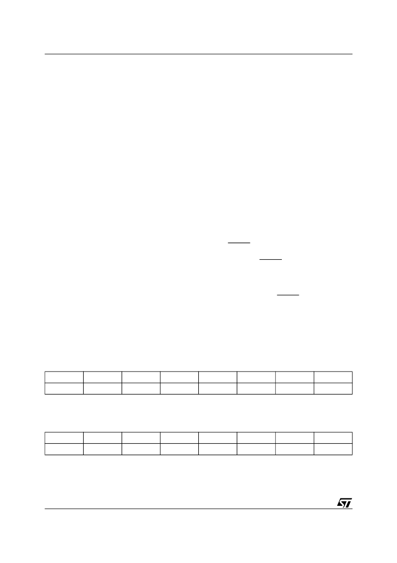
Table 11. Sector Protection/Security Bit Definition – Flash Protection Register
Note: 1. Bit Definitions:
Sec<i>_Prot
1 = Primary Flash memory or secondary Flash memory Sector <i> is write protected.
Sec<i>_Prot
0 = Primary Flash memory or secondary Flash memory Sector <i> is not write protected.
Table 12. Sector Protection/Security Bit Definition – PSD/EE Protection Register
Note: 1. Bit Definitions:
Sec<i>_Prot
1 = Secondary Flash memory Sector <i> is write protected.
Sec<i>_Prot
0 = Secondary Flash memory Sector <i> is not write protected.
Security_Bit
0 = Security Bit in device has not been set.
1 = Security Bit in device has been set.
Bit 7
Bit 6
Bit 5
Bit 4
Bit 3
Bit 2
Bit 1
Bit 0
Sec7_Prot
Sec6_Prot
Sec5_Prot
Sec4_Prot
Sec3_Prot
Sec2_Prot
Sec1_Prot
Sec0_Prot
Bit 7
Bit 6
Bit 5
Bit 4
Bit 3
Bit 2
Bit 1
Bit 0
Security_Bit
not used
not used
not used
Sec3_Prot
Sec2_Prot
Sec1_Prot
Sec0_Prot
相关PDF资料 |
PDF描述 |
|---|---|
| PSD8544V15JIT | Flash In-System Programmable ISP Peripherals For 8-bit MCUs |
| PSD9544V15JIT | Flash In-System Programmable ISP Peripherals For 8-bit MCUs |
| PSD8343V15MIT | Flash In-System Programmable ISP Peripherals For 8-bit MCUs |
| PSD9343V15MIT | 3.3V, Wide Bandwidth, 4-Channel, 2:1 Mux/DeMux Video Switch with Single Enable |
| PSD8543V15MIT | Flash In-System Programmable ISP Peripherals For 8-bit MCUs |
相关代理商/技术参数 |
参数描述 |
|---|---|
| PSD954F2-90J | 功能描述:SPLD - 简单可编程逻辑器件 U 511-PSD854F2-90J RoHS:否 制造商:Texas Instruments 逻辑系列:TICPAL22V10Z 大电池数量:10 最大工作频率:66 MHz 延迟时间:25 ns 工作电源电压:4.75 V to 5.25 V 电源电流:100 uA 最大工作温度:+ 75 C 最小工作温度:0 C 安装风格:Through Hole 封装 / 箱体:DIP-24 |
| PSD954F2-90M | 功能描述:SPLD - 简单可编程逻辑器件 U 511-PSD854F2-90M RoHS:否 制造商:Texas Instruments 逻辑系列:TICPAL22V10Z 大电池数量:10 最大工作频率:66 MHz 延迟时间:25 ns 工作电源电压:4.75 V to 5.25 V 电源电流:100 uA 最大工作温度:+ 75 C 最小工作温度:0 C 安装风格:Through Hole 封装 / 箱体:DIP-24 |
| PSD954F2V-90J | 功能描述:SPLD - 简单可编程逻辑器件 5.0V 2M 90ns RoHS:否 制造商:Texas Instruments 逻辑系列:TICPAL22V10Z 大电池数量:10 最大工作频率:66 MHz 延迟时间:25 ns 工作电源电压:4.75 V to 5.25 V 电源电流:100 uA 最大工作温度:+ 75 C 最小工作温度:0 C 安装风格:Through Hole 封装 / 箱体:DIP-24 |
| PSD954F2V-90M | 功能描述:SPLD - 简单可编程逻辑器件 PQFP-52 3V 2M 90NS RoHS:否 制造商:Texas Instruments 逻辑系列:TICPAL22V10Z 大电池数量:10 最大工作频率:66 MHz 延迟时间:25 ns 工作电源电压:4.75 V to 5.25 V 电源电流:100 uA 最大工作温度:+ 75 C 最小工作温度:0 C 安装风格:Through Hole 封装 / 箱体:DIP-24 |
| PS-DA0104-01 | 制造商:POWER-SYSTEMS 制造商全称:Power Systems GmbH+Co.KG 功能描述:DC-AC INVERTER UNIT 4 W SINGLE OUTPUTS |
发布紧急采购,3分钟左右您将得到回复。