- 您现在的位置:买卖IC网 > PDF目录69137 > PSK5A18-2B (POWER-ONE INC) 1-OUTPUT DC-DC REG PWR SUPPLY MODULE PDF资料下载
参数资料
| 型号: | PSK5A18-2B |
| 厂商: | POWER-ONE INC |
| 元件分类: | 电源模块 |
| 英文描述: | 1-OUTPUT DC-DC REG PWR SUPPLY MODULE |
| 封装: | METAL, CASE K01, MODULE |
| 文件页数: | 13/15页 |
| 文件大小: | 311K |
| 代理商: | PSK5A18-2B |
PSS, PSK Extended Data Sheet
Positive Switching Regulators (Benign)
REV. FEB 15, 2004
Page 7 of 15
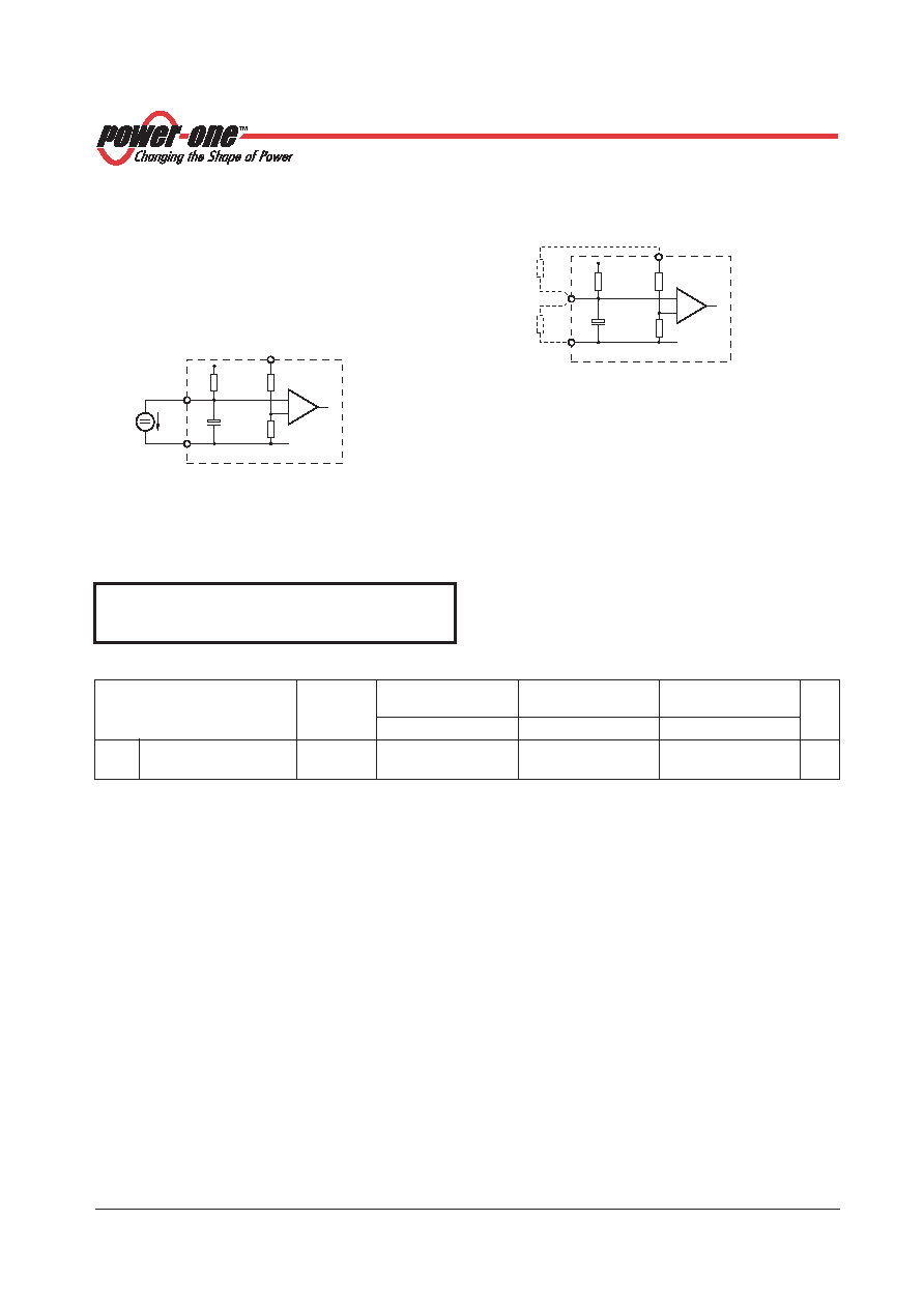
R Control
for Output Voltage Adjustment
Note: With open R input,
Vo
≈ Vo nom.
The output voltage
Vo can either be adjusted with an exter-
nal reference voltage (
Vext) or with an external resistor (R1
or
R2). The adjustment range is 0 - Vo max. The minimum dif-
ferential voltage
DVio min between input and output (see:
Electrical Input Data) should be maintained. Undervoltage
lock-out = minimum input voltage.
S+
R
+
4000
Vref
Vext
–
+
S–
06048
S+
R
–
+
4000
Uref
R1
R2
S–
06049
Fig. 9
Voltage adjustment with Vext between R and S–
a)
Vo = 0 - Vo max, using Vext between R and S–:
Vo
Vext
≈ 2.5 V –––––
Vo
≈ Vo nom –––––
Vonom
2.5 V
Fig. 10
Voltage adjustment with external resistor R1 or R2
b)
Vo = 0 - 100% Vo nom, using R1 between R and S–:
4000
Vo
Vo nom R1
R1
≈ –––––––––––
Vo
≈ –––––––––––
Vonom – Vo
R1 + 4000
c)
Vo = Vo nom - Vo max, using R2 between R and S+:
4000
Vo (Vo nom – 2.5 V)
R2
≈ ––––––––––––––––––––––––
2.5 V (
Vo – Vo nom)
Vo nom 2.5 V R2
Vo
≈ ––––––––––––––––––––––––––––––––
2.5 V (
R2 + 4000
) – Vo nom 4000
Caution: To prevent damage
Vext should not exceed
20 V, nor be negative, and
R2 should never be less than
47 k
.
Table 6: Maximum adjustable output voltage
PSS 5A14
PSS 1214
PSS 2414
PSK 5A18
PSK 1218
PSK 2418
Characteristics
Conditions
min
typ
max
min
typ
max
min
typ
max
Unit
Vo max Maximum adjustable
Vi nom, Io nom
5.6
16.0
26.0
V
output at R control input
CS
Current Sharing
For parallel operation of several modules, interconnecting
all CS pins ensures that the output currents are evenly dis-
tributed. This feature improves transient load performance
and increases system reliability. All paralleled units should
be
supplied
by
equal
input
voltage
(
Vi)
and
interconnecting leads should have equal length and cross
section to ensure equal voltage drop.
相关PDF资料 |
PDF描述 |
|---|---|
| PSS129-7EPCB1 | 1-OUTPUT 108 W DC-DC REG PWR SUPPLY MODULE |
| PSS249-9EPCB1 | 1-OUTPUT DC-DC REG PWR SUPPLY MODULE |
| PSK3612-9EPCB | 1-OUTPUT DC-DC REG PWR SUPPLY MODULE |
| PSK4812-7EPCB1 | 1-OUTPUT 576 W DC-DC REG PWR SUPPLY MODULE |
| PSS249-7EPCB | 1-OUTPUT DC-DC REG PWR SUPPLY MODULE |
相关代理商/技术参数 |
参数描述 |
|---|---|
| PSK5A20-7 | 功能描述:SWITCHING REGULATOR 102W 5.1V RoHS:是 类别:电源 - 板载 >> DC DC Converters 系列:* 标准包装:5 系列:* |
| PSK5A20-9 | 制造商:Power-One 功能描述:DCDC - Bulk |
| PSK5A25-7 | 功能描述:SWITCHING REGULATOR 127.5W 5.1V RoHS:是 类别:电源 - 板载 >> DC DC Converters 系列:* 标准包装:5 系列:* |
| PSK5A25-9 | 制造商:Power-One 功能描述:DCDC - Bulk |
| PSK645I | 制造商:Panduit Corp 功能描述:UNIVERSAL STRUT CLAMP FOR 4 EMT/RIGID/I 制造商:Panduit Corp 功能描述:UNIVERSAL STRUT CLAMP FOR 4 CONDUIT |
发布紧急采购,3分钟左右您将得到回复。