- 您现在的位置:买卖IC网 > PDF目录69128 > PSL486-7LIRPCDA 1-OUTPUT DC-DC REG PWR SUPPLY MODULE PDF资料下载
参数资料
| 型号: | PSL486-7LIRPCDA |
| 元件分类: | 电源模块 |
| 英文描述: | 1-OUTPUT DC-DC REG PWR SUPPLY MODULE |
| 文件页数: | 11/11页 |
| 文件大小: | 247K |
| 代理商: | PSL486-7LIRPCDA |
PSL-Family
Switching Regulators 19"
Rugged Environment
5 - 10
Edition 2/96 - Melcher AG
MELCHER
The Power Partners.
5.1
Option -9 Extended Temperature Range
The operational ambient temperature range is extended to
TA = –40...71
°C.
Option P Potentiometer
Option P and the R-function cannot be supported simulta-
neously. The output voltage
Uo can be adjusted with a
screwdriver in the range from 0.92...1.08 of the nominal
output voltage
Uo nom.
However, the minimum differential voltage
U
i o min between
input and output voltages as specified in "Electrical Input
and Output Data" should be maintained.
Option U Ambient Temp. Range acc. UL Recognition
Underwriters Laboratories (UL) have approved the PSL
family as recognized components up to an ambient tem-
perature of
T
A max – 10 K given by the upper temperature
limit of the standard PCB material. If the full maximum am-
bient temperature
T
A max is required with UL approval, op-
tion U should be requested. It consists of an alternative
PCB material with a higher maximum temperature specifi-
cation.
The European approval boards have in contrast to UL ac-
cepted the standard PCB material to be operated up to
TA max = 71°C without any further precautions.
Option L Input filter
Option L is recommended to reduce superimposed inter-
ference voltages, and to prevent oscillations, if input lines
exceed approx. 5 m in total length. The fundamental wave
(approx. 120 kHz) of the reduced interference voltage be-
tween Vi+ and Gi– has, with an input line inductance of
5
H a maximum magnitude of 4 mVrms.
The input impedance of the switching regulator at 120 kHz
is about 50 m
. The harmonics are small in comparison
with the fundamental wave. See also data: RFI.
With option L, the maximum permissible additionally super-
imposed ripple
ui of the input voltage (rectifier mode) at a
specified input frequency
f i has the following values:
ui max = 10 Vpp at 100 Hz or Vpp = 1000 Hz/fi 1 V
Option C
Thyristor Crowbar
This option is recommended to protect the load against
power supply malfunction, but it is not designed to sink ex-
ternal currents.
A fixed-value monitoring circuit checks the output voltage
Uo. When the trigger voltage Uoc is reached, the thyristor
crowbar triggers and disables the output. It may be deacti-
vated by removal of the input voltage. In case of a switching
transistor defect, an internal fuse prevents excessive cur-
rent.
Note: As a central overvoltage protection device, the crow-
bar is usually connected to the external load via distributed
inductance of the lines. For this reason, the overvoltage at
the load can temporarily exceed the trigger voltage
Uoc. De-
pending on the application, further decentralized over-
voltage protection elements may have to be used addition-
ally.
Table 10: Crowbar trigger levels
Characteristics
Conditions
12 V
15 V
24 V
36 V
48 V
Unit
min
max
min
max
min
max
min
max
min
max
Uo c
Trigger voltage
Ui min...Ui max
13.5
16
16.5
19
27
31
40
45.5
55
60
V
Io = 0...Io nom
t s
Delay time
TC min...TC max
1.5
s
Option D “Save Data”, input undervoltage monitor
Note: Output instead of input undervoltage monitor is
available on request (option D1).
If the input voltage
Ui is below the adjustable threshold volt-
age
Ut, the control circuit for terminal D has low impedance.
Terminal D and Go– are connected to a self-conducting
field effect transistor (FET). A 0.5 W Zener diode provides
protection against overvoltages.
The voltage
Ut can be externally adjusted with a trim poten-
tiometer by means of a screwdriver. The hysteresis
UH of
Ut is <2 %. Terminal D stays low for a minimum time
tlow min, in order to prevent any oscillation. Ut can be set to a
value between
Ui min and Ui max according to fig. 10. It is im-
portant to note that the FET can become conductive again
when
UD > Ui – 3V.
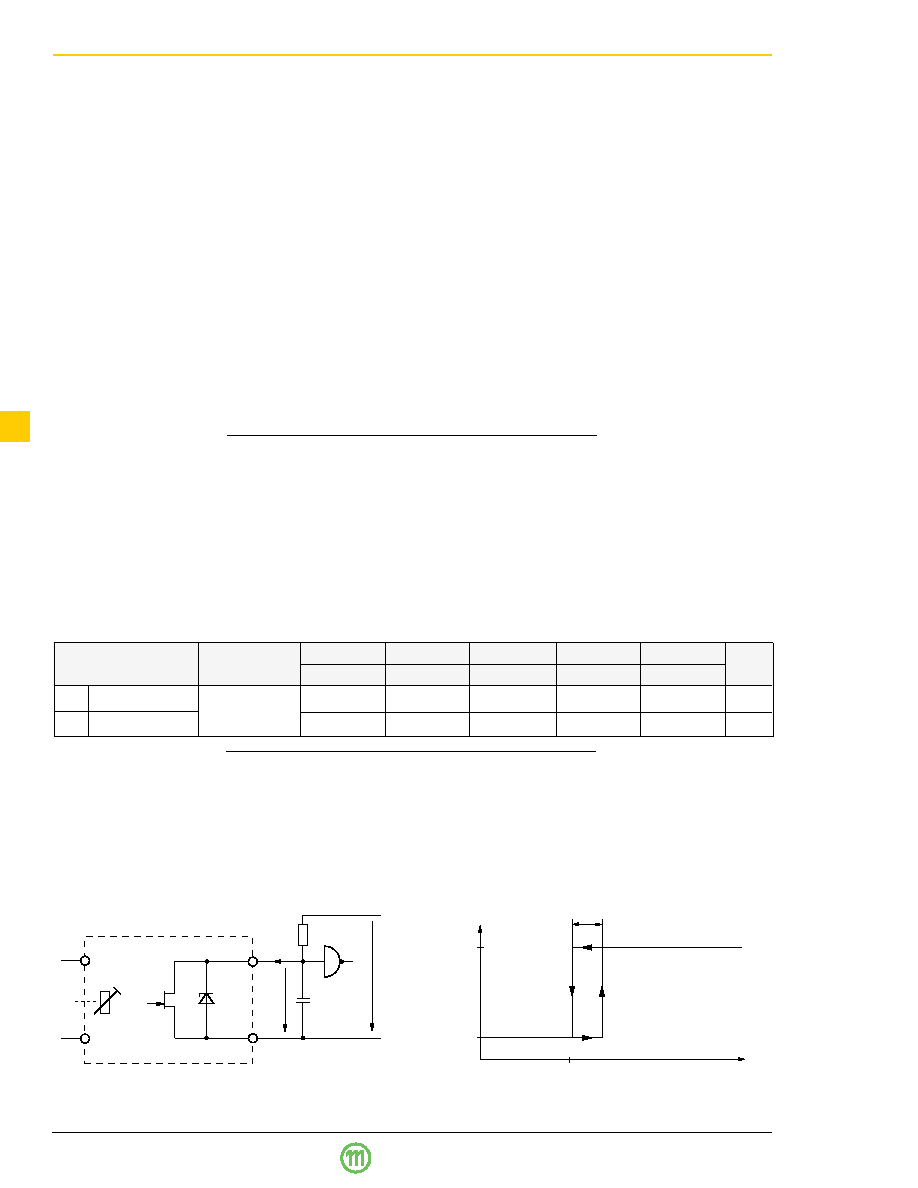
Fig. 11
Test circuit with definition of voltage UD and current ID on
Terminal D.
Fig. 12
Definition of Ut and UH
Vi +
Gi –
Go –
8.2 V
D
UD
+5 V
100 pF
ID
10 k
FET
Ut
UD
UD high
UD low
Ut
Ui
UH
相关PDF资料 |
PDF描述 |
|---|---|
| PSL486-9LIRPCDA | 1-OUTPUT DC-DC REG PWR SUPPLY MODULE |
| PSL486-7IPCDA | 1-OUTPUT DC-DC REG PWR SUPPLY MODULE |
| PSL156-9LIRPCDA | 1-OUTPUT DC-DC REG PWR SUPPLY MODULE |
| PSL156-7RCDA | 1-OUTPUT DC-DC REG PWR SUPPLY MODULE |
| PSL486-9LIRPCDA | 1-OUTPUT DC-DC REG PWR SUPPLY MODULE |
相关代理商/技术参数 |
参数描述 |
|---|---|
| PSL486-7LR | 制造商:Power-One 功能描述: |
| PSL486-7R | 功能描述:SWITCHING REGULATOR 288W 48V RoHS:是 类别:电源 - 板载 >> DC DC Converters 系列:* 标准包装:5 系列:* |
| PSL486-9R | 制造商:Power-One 功能描述:DC/DC PS SGL-OUT 48V 6A 288W 11PIN - Bulk |
| PSL-4BLK | 制造商:Panduit Corp 功能描述:XENOY PADLOCK, 1.50" BODY, BLACK - Bag 制造商:Panduit Corp 功能描述:Safety Lockout Padlocks |
| PSL-4BLK-LB | 制造商:Panduit Corp 功能描述:Safety Lockout Padlocks 制造商:Panduit Corp 功能描述:XENOY PADLOCK, 3.00" BODY, BLACK - Bag |
发布紧急采购,3分钟左右您将得到回复。