- 您现在的位置:买卖IC网 > PDF目录66039 > PT5022L (TEXAS INSTRUMENTS INC) 1 A SWITCHING REGULATOR, 1200 kHz SWITCHING FREQ-MAX, SMA3 PDF资料下载
参数资料
| 型号: | PT5022L |
| 厂商: | TEXAS INSTRUMENTS INC |
| 元件分类: | 稳压器 |
| 英文描述: | 1 A SWITCHING REGULATOR, 1200 kHz SWITCHING FREQ-MAX, SMA3 |
| 封装: | ROHS COMPLIANT, SMD-3 |
| 文件页数: | 1/6页 |
| 文件大小: | 131K |
| 代理商: | PT5022L |
For technical support and more information, see inside back cover or visit www.ti.com
Ordering Information
PT5021
o = -3.3 Volts
PT5022
o = -5 Volts
PT5023
o = -9 Volts
PT5024
o = -12 Volts
PT5025
o = -15 Volts
PT5026
o = -5.2 Volts
PT5027
o = -8.0 Volts
PT5028
o = -6.5 Volts
PT5029
o = -5.5 Volts
PT5030
o = -6.0 Volts
PT5031
o = -1.7 Volts
Pin
Function
1Vin
2
GND
3Vout
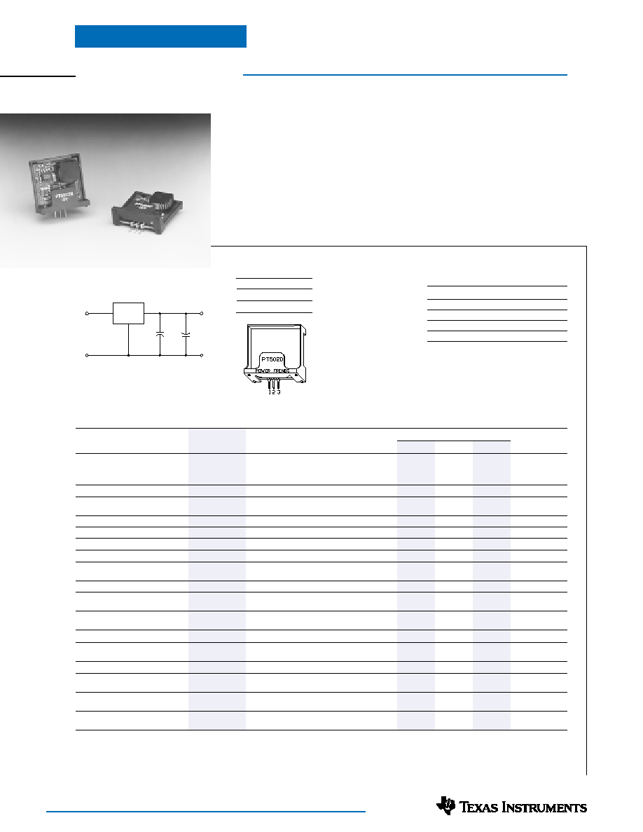
Standard Application
C1 = Optional ceramic (1-5F)
C2 = Required Electrolytic (100F)
Features
Negative Output
Input Voltage Range:
+4.75 to +7 Volts
Laser-Trimmed
Small Footprint
Soft Start
5-Pin Mount Option
(Suffixes L & M)
Description
The PT5020 series of integrated
switching regulators (ISRs) convert a
positive input voltage, typically +5V, to a
negative output voltage for a wide range of
analog and datacom applications.
These Plus to Minus ISRs incorporate
a “Buck-Boost” topology and are packaged
in the 3-pin, single in-line pin (SIP)
package configuration.
NOTE: PT5020 ISRs are not Short-Circuit Protected.
Positive Input/Negative Output
Integrated Switching Regulator
PT5020 Series
Pin-Out Information
SLTS025B
(Revised 12/19/2001)
PT Series Suffix (PT1234x )
Case/Pin
Order
Package
Configuration
Suffix
Code *
Vertical
N
(EAD)
Horizontal
A
(EAA)
SMD
C
(EAC)
Horizontal, 2-pin Tab
M
(EAM)
SMD, 2-Pin Tab
L
(EAL)
* Previously known as package styles 100/110.
(Reference the applicable package code drawing
for the dimensions and PC board layout)
PT5020
3
2
1
C
2
100F +
C
1
–V
out
COM
+V
in
Specifications (Unless otherwise stated, Ta =25°C, Vin =5V, Io =Iomax, C2 =100F)
PT5020 SERIES
Characteristics
Symbol
Conditions
Min
Typ
Max
Units
Output Current
Io
Over Vin range
Vo= –1.7V to –6.5V
0.25 (1)
—
1.0
Vo= –9V
0.10 (1)
—0.60
A
Vo= –12V
0.10 (1)
—0.50
Vo= –15V
0.10 (1)
—0.30
Input Voltage Range
Vin
Over Io range
4.75
—
7 (2)
V
Output Voltage Tolerance
Vo
Over Vin Range
—
±1.5
±3
%Vo
Ta = -20°C to SOA limit (3)
Line Regulation
Regline
Over Vin range
—
±0.5
±1
%Vo
Load Regulation
Regload
Iomin ≤ Io ≤ Iomax
—
±0.5
±1
%Vo
Efficiency
η
Io =0.5 Iomax
—
75
—
%
Vo Ripple (pk-pk)
Vr
20MHz bandwidth
—
±2
±5
%Vo
Transient Response
ttr
25% load change
—
500
—
Sec
Vo over/undershoot
—
3.0
5.0
%Vo
Current Limit
Ilim
—150
—
%Iomax
Inrush Current
Iir
On start up
—
1.0 (3)
—A
tir
—
1.0
—
mSec
Switching Frequency
s
Over Io range
Vo =1.7 to 8V
0.8
1
1.2
MHz
Vo ≥8 V
500
650
800
kHz
Operating Temperature Range
Ta
—
-20
—
+85 (4)
°C
Thermal Resistance
θ
ja
Free Air Convection
—
50
—
°C/W
(40-60LFM)
Storage Temperature
Ts
-40
—
+125
°C
Mechanical Shock
Per Mil-STD-883D, Method 2002.3
—
500
—
G’s
1 msec, Half Sine, mounted to a fixture
Mechanical Vibration
Suffixes N, A, & C
—
5
—
G’s
Per Mil-STD-883D, 20-2000 Hz
Suffixes L & M
—
20
—
Weight
Suffixes N, A, & C
—
4.5
—
grams
Suffixes L & M
—
6.5 (5)
—
Notes:
(1) The ISR will operate at no load with reduced specifications.
(2) For applications with input voltages greater than 7 VDC, use the PT78NR100 Series.
(3) The inrush current stated is above the normal input current for the associated output load.
(4) See Safe Operating Area curves or consult the factory for the appropriate derating
(5) The tab pins on the 5-pin mount package types (suffixes L & M) must be soldered. For more information see the applicable package outline drawing.
相关PDF资料 |
PDF描述 |
|---|---|
| PT5027N | SWITCHING REGULATOR, SMA3 |
| PT5021C | SWITCHING REGULATOR, SMA3 |
| PT5028N | SWITCHING REGULATOR, SMA3 |
| PT5027A | SWITCHING REGULATOR, SMA3 |
| PT5022C | SWITCHING REGULATOR, SMA3 |
相关代理商/技术参数 |
参数描述 |
|---|---|
| PT5022LT | 功能描述:REGLTR -5V 1A 3PIN HS SMD T/R RoHS:是 类别:电源 - 板载 >> DC DC Converters 系列:PT5020 标准包装:10 系列:PT4570 类型:隔离 输出数:1 电压 - 输入(最小):36V 电压 - 输入(最大):75V Voltage - Output 1:9V Voltage - Output 2:- Voltage - Output 3:- 电流 - 输出(最大):3.3A 电源(瓦) - 制造商系列:30W 电压 - 隔离:1.5kV(1500V) 特点:- 安装类型:表面贴装 封装/外壳:19-SIP SMD 模块 尺寸/尺寸:3.00" L x 1.19" W x 0.50" H(76.2mm x 30.2mm x 12.7mm) 包装:托盘 工作温度:-40°C ~ 85°C 效率:84% 电源(瓦特)- 最大:30W |
| PT5022M | 功能描述:DC/DC转换器 -5Vout 1A +5V-In Pos-Neg ISR RoHS:否 制造商:Murata 产品: 输出功率: 输入电压范围:3.6 V to 5.5 V 输入电压(标称): 输出端数量:1 输出电压(通道 1):3.3 V 输出电流(通道 1):600 mA 输出电压(通道 2): 输出电流(通道 2): 安装风格:SMD/SMT 封装 / 箱体尺寸: |
| PT5022N | 功能描述:DC/DC转换器 -5Vout 1A +5V-In Pos-Neg ISR RoHS:否 制造商:Murata 产品: 输出功率: 输入电压范围:3.6 V to 5.5 V 输入电压(标称): 输出端数量:1 输出电压(通道 1):3.3 V 输出电流(通道 1):600 mA 输出电压(通道 2): 输出电流(通道 2): 安装风格:SMD/SMT 封装 / 箱体尺寸: |
| PT5022S | 功能描述:开关变换器、稳压器与控制器 -5Vout 1A +5V-In Pos-Neg ISR RoHS:否 制造商:Texas Instruments 输出电压:1.2 V to 10 V 输出电流:300 mA 输出功率: 输入电压:3 V to 17 V 开关频率:1 MHz 工作温度范围: 安装风格:SMD/SMT 封装 / 箱体:WSON-8 封装:Reel |
| PT5023 | 制造商:Pulse Electronics Corporation 功能描述:T1/E1, SGL, THT, XFMR |
发布紧急采购,3分钟左右您将得到回复。