- 您现在的位置:买卖IC网 > PDF目录69251 > PT8103C (TEXAS INSTRUMENTS INC) 39 A SWITCHING REGULATOR, 400 kHz SWITCHING FREQ-MAX, MSMA31 PDF资料下载
参数资料
| 型号: | PT8103C |
| 厂商: | TEXAS INSTRUMENTS INC |
| 元件分类: | 稳压器 |
| 英文描述: | 39 A SWITCHING REGULATOR, 400 kHz SWITCHING FREQ-MAX, MSMA31 |
| 封装: | METAL, SMD-31 |
| 文件页数: | 11/14页 |
| 文件大小: | 241K |
| 代理商: | PT8103C |
For technical support and more information, see inside back cover or visit www.ti.com
6
PT8100 Series
40-A 3.3/5-V Input Programmable
Integrated Switching Regulator
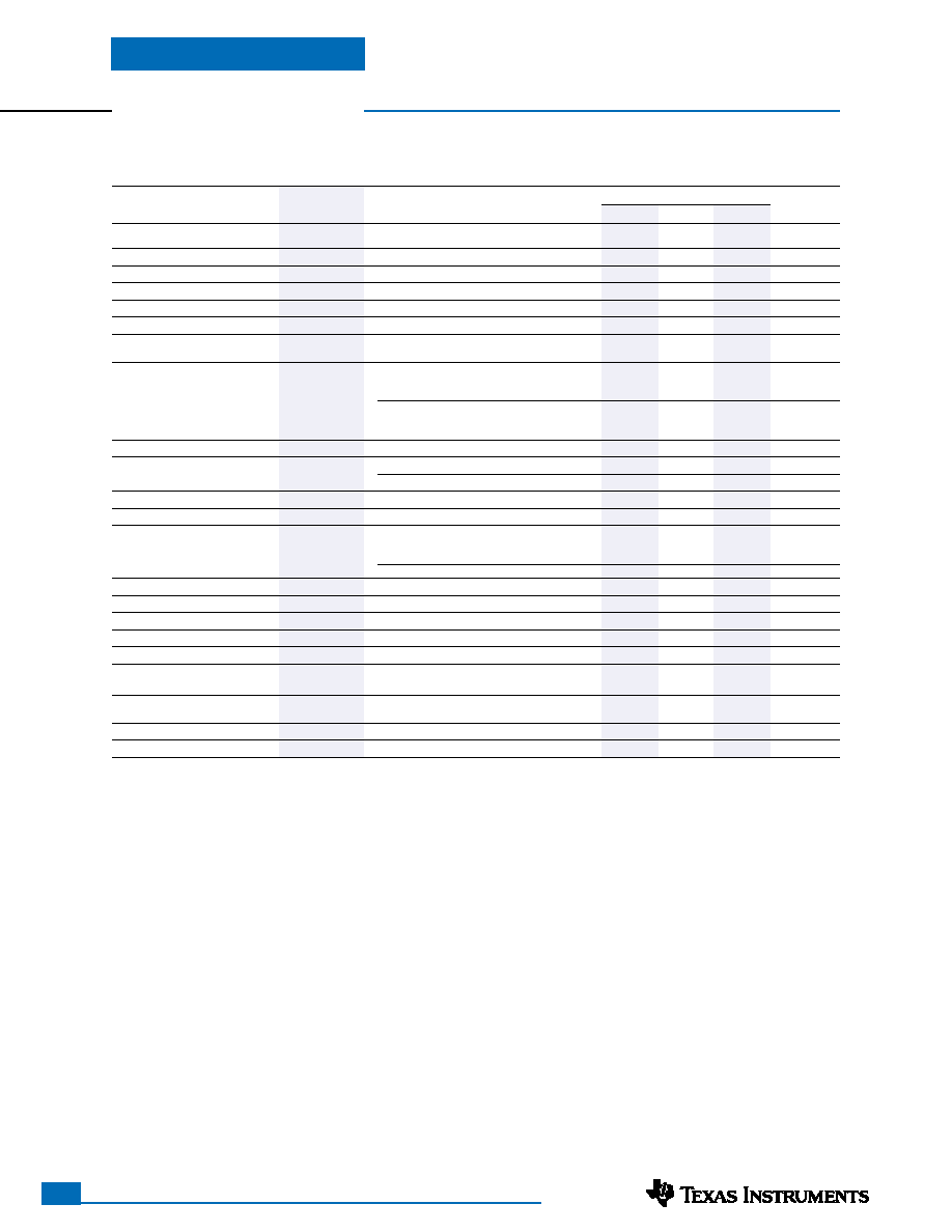
PT8104 Specifications (Unless otherwise stated Ta =25°C, C1 =1,500F, C2 =660F, Vin =5V, Vo =1.8V, & Io =40A )
PT8104, Vin =5V
Characteristics
Symbols
Conditions
Min
Typ
Max
Units
Output Current
Io
25°C, natural convection
0.1 (1)
—38
A
60°C with 200LFM airflow
0.1 (1)
—40
Input Voltage Range
Vin
Over Io Range
4.5
—
5.5
V
Set-Point Voltage Tolerance
Vo tol
Over Vo range
—
±1
±2
%V
Line Regulation
Regline
Over Vin range
—
±10
—
mV
Load Regulation (Droop)
Regload
Over Io range
—
1.5
—
mV/A
Temperature Variation
Regtemp
–40°C
≤Ta ≤85°C
—
±0.5
—
%Vo
Total Output Voltage Variation
Votot
Includes set-point, line, load,
—
75 (2)
mV
–40°C
≤Ta ≤ 85°C, pin 31 to GND
Efficiency
η
Io =15A
Vo =1.8V
—
90
—
Vo =1.5V
—
88
—
%
Vo =1.2V
—
87
—
Io =40A
Vo =1.8V
—
85
—
Vo =1.5V
—
82
—
%
Vo =1.2V
—
80
—
Vo Ripple (pk-pk)
Vr
20MHz bandwidth
—
25
—
mV
Transient Response (Vo =1.2V)
ttr
1A/s load step, 50% to 100% Iomax
—
50
—
Sec
Vtr
Vo over/undershoot
—
50
—
mV
Short Circuit Threshold
Iosc
—
58
—
A
Switching Frequency
o
Over load range
300
350
400
kHz
Standby Control (pin 6)
Input High Voltage
VIH
Referenced to GND (pins 17–22)
—
Open (3)
V
Input Low Voltage
VIL
–0.2
—
0.8
Input Low Current
IIL
Pin 6 to GND
—
0.5
—
mA
Standby Input Current
Iin standby
Pin 6 to GND
—
35
—
mA
External Output Capacitance
C2
See PT8104 application schematic
660 (6)
—
15,000
F
External Input Capacitance
C1
See PT8104 application schematic
1,500
—
F
Operating Temperature Range
Ta
Over Vin Range
–40 (4)
—+85 (5)
°C
Storage Temperature
Ts
—
–40
—
+125
°C
Mechanical Shock
Per Mil-STD-883D, Method 2002.3
1 msec, Half Sine, mounted to a fixture
—
500
—
G’s
Mechanical Vibration
Mil-STD-883D, Method 2007.2
Vertical
—
20 (7)
—
G’s
20-2000 Hz, soldered in PCB
Horizontal
—
20 (7)
Weight
—
Vertical/Horizontal
—
55
—
grams
Flammability
—
Materials meet UL 94V-0
Notes: (1) ISR-will operate down to no load with reduced specifications.
(2) Total output voltage variation includes load regulation droop, which is required for compliance with specification VRM 8.4-5
(3) The Standby input (pin 6) has an internal pull-up. If it is left open-circuit the module will operate when input power is applied. A low-leakage
MOSFET is recommended to control this input. The open-circuit voltage is nominally 5V. See application notes for interface considerations.
(4) For operation below 0°C, Cout must have stable characteristics. Use either low ESR tantalum or Oscon capacitors.
(5) See safe Operating Area curves or consult factory for the appropriate derating.
(6) The PT8100 regulators require a minimum of 660F, low ESR ouput capacitance (1,200F for standard aluminum electrolytic) for proper operation.
(7) The case pins on the through-hole package types (suffixes N & A) must be soldered. For more information see the applicable package outline drawing.
Input Filter: The filter components L1 and C3 are optional for most applications. The inductor must be rated to handle the projected input current. A rating of 20ADC is
recommended. The input capacitance, C1 must be rated for a minimum of 1Arms of ripple current. For transient or dynamic load applications, additional capacitance
may be required. For more information refer to the application note on capacitor recommendations for this product.
相关PDF资料 |
PDF描述 |
|---|---|
| PT8102C | 38 A SWITCHING REGULATOR, 400 kHz SWITCHING FREQ-MAX, MSMA31 |
| PT8103A | 39 A SWITCHING REGULATOR, 400 kHz SWITCHING FREQ-MAX, MSMA31 |
| PT8101N | 38 A SWITCHING REGULATOR, 400 kHz SWITCHING FREQ-MAX, MSMA31 |
| PT8104C | 38 A SWITCHING REGULATOR, 400 kHz SWITCHING FREQ-MAX, MSMA31 |
| PT8102N | 38 A SWITCHING REGULATOR, 400 kHz SWITCHING FREQ-MAX, MSMA31 |
相关代理商/技术参数 |
参数描述 |
|---|---|
| PT8103N | 功能描述:开关变换器、稳压器与控制器 1.075-1.85V 40A 3.3V Inp Multiph Prog ISR RoHS:否 制造商:Texas Instruments 输出电压:1.2 V to 10 V 输出电流:300 mA 输出功率: 输入电压:3 V to 17 V 开关频率:1 MHz 工作温度范围: 安装风格:SMD/SMT 封装 / 箱体:WSON-8 封装:Reel |
| PT8104 | 制造商:TI 制造商全称:Texas Instruments 功能描述:40-A 3.3/5-V Input Programmable Integrated Switching Regulator |
| PT8104A | 功能描述:REGULATOR 5VIN 40A HORZ RoHS:否 类别:电源 - 板载 >> DC DC Converters 系列:PT8100 设计资源:Maxi/Mini/Micro Design Guide, Appl Manual 标准包装:1 系列:Maxi 类型:隔离 输出数:1 电压 - 输入(最小):43V 电压 - 输入(最大):110V Voltage - Output 1:15V Voltage - Output 2:- Voltage - Output 3:- 电流 - 输出(最大):* 电源(瓦) - 制造商系列:400W 电压 - 隔离:* 特点:* 安装类型:通孔 封装/外壳:模块 尺寸/尺寸:4.60" L x 2.20" W x 0.54" H(116.8mm x 55.9mm x 13.7mm) 包装:散装 工作温度:-55°C ~ 100°C 效率:* 电源(瓦特)- 最大:* |
| PT8104C | 制造商:TI 制造商全称:Texas Instruments 功能描述:40-A 3.3/5-V Input Programmable Integrated Switching Regulator |
| PT8104N | 制造商:TI 制造商全称:Texas Instruments 功能描述:40-A 3.3/5-V Input Programmable Integrated Switching Regulator |
发布紧急采购,3分钟左右您将得到回复。