- 您现在的位置:买卖IC网 > PDF目录69251 > PTB48501AAZ (TEXAS INSTRUMENTS INC) 2-OUTPUT 32.4 W DC-DC REG PWR SUPPLY MODULE PDF资料下载
参数资料
| 型号: | PTB48501AAZ |
| 厂商: | TEXAS INSTRUMENTS INC |
| 元件分类: | 电源模块 |
| 英文描述: | 2-OUTPUT 32.4 W DC-DC REG PWR SUPPLY MODULE |
| 封装: | ROHS COMPLIANT PACKAGE-10 |
| 文件页数: | 4/18页 |
| 文件大小: | 400K |
| 代理商: | PTB48501AAZ |
www.ti.com
SWITCHING FREQUENCY SYNCHRONIZATION
POWER-UP SEQUENCING
CONFIGURING THE PTB4850X AND
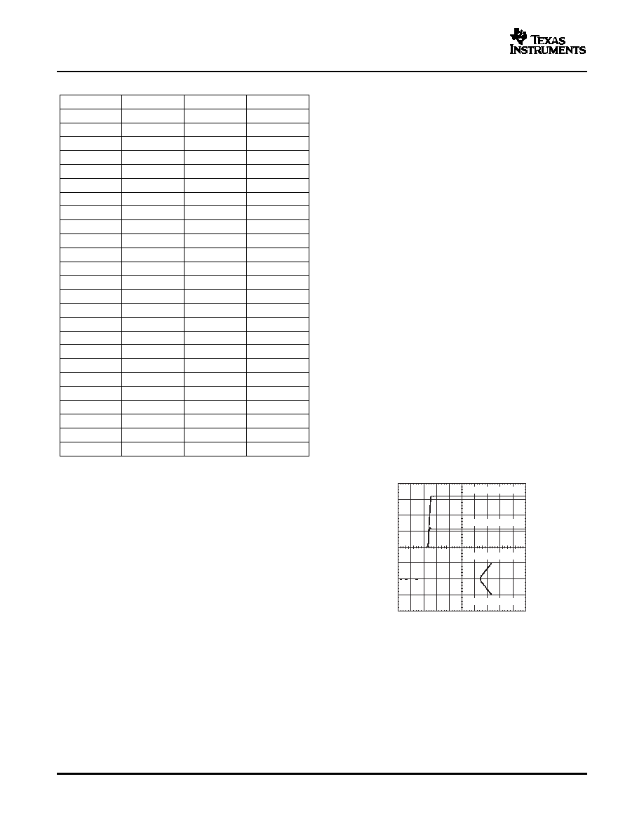
HORIZ SCALE: 10 ms/Div
VCCIO (1 V/div)
VCORE (1 V/div)
+VTCVR (5 V/div)
VTCVR (5 V/div)
SLTS218C – SEPTEMBER 2003 – REVISED AUGUST 2006
Table 2. Adjust Resistor Values (continued)
Part No.
PTB4850xA
PTB48502A
Unsynchronized, the difference in switch frequency
introduces a beat frequency into the input and output
% Adjust
Va (V)
R1 / (R2)(1)
AC ripple components from the converters. The beat
–13
1.044
(12.7) k
(11.1) k
frequency can vary considerably with any slight
–12
1.056
(15.7) k
(13.4) k
variation in either converter's switch frequency. This
–11
1.068
(19.2) k
(16.1) k
results in a variable and undefined frequency
–10
1.080
(23.4) k
(19.4) k
spectrum for the ripple waveforms, which would
normally require separate filters at the input of each
– 9
1.092
(28.6) k
(23.4) k
converter.
When
the
switch
frequency
of
the
– 8
1.104
(35) k
(28.4) k
converters are synchronized, the ripple components
–7
1.116
(43.2) k
(34.8) k
are constrained to the fundamental and higher. This
–6
1.128
(54.2) k
(43.4) k
simplifies the design of the output filters, and allows
–5
1.140
(69.7) k
(55.4) k
a common filter to be specified for the treatment of
input ripple.
–4
1.152
(92.8) k
(73.4) k
–3
1.164
(131) k
103.0) k
–2
1.176
(208) k
163.0) k
The desired power-up sequence for the AC7 supply
–1
1.188
(440) k
343.0) k
voltages requires that the two logic-level voltages
0
1.200
from the PTB4850x converter rise to regulation prior
+ 1
1.212
148 k
108.0 k
to the two complementary voltages that power the
+ 2
1.224
65.8 k
48.0 k
transceiver
ICs.
This
sequence
cannot
be
guaranteed if the PTB4850x and PTB4851x are
+ 3
1.236
38.4 k
28.1 k
allowed to power up independently, especially if the
+ 4
1.248
24.6 k
18.1 k
48-V input voltage rises relatively slowly. To ensure
+ 5
1.260
16.4 k
12.1 k
the desired power-up sequence, the EN Out pin of
+ 6
1.272
10.9 k
8.1 k
the PTB4850x is directly connected to the activelow
+ 7
1.284
7 k
5.3 k
Enable input of the PTB4851x (see Figure 20). This
allows the PTB4850x to momentarily hold off the
+ 8
1.296
4.1 k
3.2 k
outputs from the PTB4851x until the logic-level
+ 9
1.308
1.8 k
1.5 k
voltages have risen first. Figure 19 shows the
+10
1.320
0 k
0.2 k
power-up waveforms of all four supply voltages from
the schematic of Figure 20.
PTB4851X FOR DSL APPLICATIONS
When operated as a pair, the PTB4850x and
PTB4851x converters are specifically designed to
provide all the required supply voltages for powering
xDSL chipsets. The PTB4850x produces two logic
voltages. They include a 3.3-V source for logic and
I/O, and a low-voltage for powering a digital signal
processor core. The PTB4851x produces a balanced
pair of complementary supply voltages that is
required for the xDSL transceiver ICs. When used
together
in
these
types
of
applications,
the
PTB4850x and PTB4851x may be configured for
power-up sequencing, and also synchronized to a
Figure 19. Power-Up Sequencing Waveforms
common switch conversion frequency. Figure 20
shows the required cross-connects between the two
converters to enable these two features.
12
相关PDF资料 |
PDF描述 |
|---|---|
| PTB48501AAS | 2-OUTPUT 32.4 W DC-DC REG PWR SUPPLY MODULE |
| PTB48501AAH | 2-OUTPUT 32.4 W DC-DC REG PWR SUPPLY MODULE |
| PTB48502AAZ | 2-OUTPUT 48.6 W DC-DC REG PWR SUPPLY MODULE |
| PTB48502AAS | 2-OUTPUT 48.6 W DC-DC REG PWR SUPPLY MODULE |
| PTB48511AAH | 2-OUTPUT 65 W DC-DC REG PWR SUPPLY MODULE |
相关代理商/技术参数 |
参数描述 |
|---|---|
| PTB48502 | 制造商:TI 制造商全称:Texas Instruments 功能描述:DUAL-OUTPUT, 48-V INPUT ISOLATED DC/DC CONVERTER for xDSL |
| PTB48502AAH | 功能描述:DC/DC转换器 3.3/1.2V 45W Out 48V Inp DC/DC Converter RoHS:否 制造商:Murata 产品: 输出功率: 输入电压范围:3.6 V to 5.5 V 输入电压(标称): 输出端数量:1 输出电压(通道 1):3.3 V 输出电流(通道 1):600 mA 输出电压(通道 2): 输出电流(通道 2): 安装风格:SMD/SMT 封装 / 箱体尺寸: |
| PTB48502AAS | 功能描述:直流/直流开关转换器 3.3/1.2V 45W Out 48V Inp DC/DC Converter RoHS:否 制造商:STMicroelectronics 最大输入电压:4.5 V 开关频率:1.5 MHz 输出电压:4.6 V 输出电流:250 mA 输出端数量:2 最大工作温度:+ 85 C 安装风格:SMD/SMT |
| PTB48502AAZ | 功能描述:DC/DC转换器 3.3/1.2V 45W Out 48V Inp DC/DC Converter RoHS:否 制造商:Murata 产品: 输出功率: 输入电压范围:3.6 V to 5.5 V 输入电压(标称): 输出端数量:1 输出电压(通道 1):3.3 V 输出电流(通道 1):600 mA 输出电压(通道 2): 输出电流(通道 2): 安装风格:SMD/SMT 封装 / 箱体尺寸: |
| PTB48510 | 制造商:TI 制造商全称:Texas Instruments 功能描述:Dual Complementary-Output DC/DC Converter for DSL |
发布紧急采购,3分钟左右您将得到回复。