- 您现在的位置:买卖IC网 > PDF目录69252 > PTH03010WAD (TEXAS INSTRUMENTS INC) 1-OUTPUT DC-DC REG PWR SUPPLY MODULE PDF资料下载
参数资料
| 型号: | PTH03010WAD |
| 厂商: | TEXAS INSTRUMENTS INC |
| 元件分类: | 电源模块 |
| 英文描述: | 1-OUTPUT DC-DC REG PWR SUPPLY MODULE |
| 封装: | ROHS COMPLIANT, DIP-10 |
| 文件页数: | 13/19页 |
| 文件大小: | 510K |
| 代理商: | PTH03010WAD |
For technical support and more information, visit http://power.ti.com
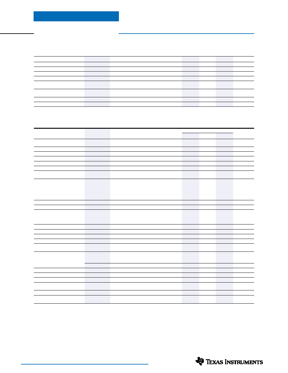
Environmental & Absolute Maximum Ratings (Voltages are with respect to GND)
Characteristics
Symbols
Conditions
Min
Typ
Max
Units
Track Input Voltage
Vtrack
–0.3
—
Vin + 0.3
V
Operating Temperature Range
Ta
Over Vin Range
–40
—
85
°C
Solder Reflow Temperature
Treflow
Surface temperature of module body or pins
235 (i)
°C
Storage Temperature
Ts
—
–40
—
125
°C
Mechanical Shock
Per Mil-STD-883D, Method 2002.3
—
500
—
G’s
1 msec, Sine, mounted
Mechanical Vibration
Mil-STD-883D, Method 2007.2
—
20
—
G’s
20-2000 Hz
Weight
—
5
—
grams
Flammability
—
Meets UL 94V-O
Notes:
(i) During reflow of SMD package version do not elevate peak temperature of the module, pins or internal components above the stated maximum.
PTH03010W —3.3-V Input
15-A, 3.3-V Input Non-Isolated
Wide-Output Adjust Power Module
SLTS203C – MAY 2003 – REVISED DECEMBER 2003
Specifications (Unless otherwise stated, Ta =25 °C, Vin =3.3 V, Vout =2 V, Cin =470 F, Cout =0 F, and Io =Iomax)
PTH03010W
Characteristics
Symbols
Conditions
Min
Typ
Max
Units
Output Current
Io
0.8 V
≤ Vo ≤ 2.5 V,
60 °C, 200 LFM airflow
0
—
15 (1)
A
25 °C, natural convection
0
—
15 (1)
Input Voltage Range
Vin
Over Io range
2.95 (2)
—
3.65
V
Set-Point Voltage Tolerance
Votol
—
±2 (3)
%Vo
Temperature Variation
Regtemp
–40 °C <Ta < +85 °C
—
±0.5
—
%Vo
Line Regulation
Regline
Over Vin range
—
±10
—
mV
Load Regulation
Regload
Over Io range
—
±12—
mV
Total Output Variation
Regtot
Includes set-point, line, load,
—
±3 (3)
%Vo
–40 °C
≤ Ta ≤ +85 °C
Efficiency
η
Io =10 A
RSET = 2.21 k Vo = 2.5 V
—
93
—
RSET = 4.12 k Vo = 2.0 V
—
92
—
RSET = 5.49 k Vo = 1.8 V
—
91
—
%
RSET = 8.87 k Vo = 1.5 V
—
89
—
RSET = 17.4 k Vo = 1.2 V
—
87
—
RSET = 36.5 k Vo = 1.0 V
—
85
—
Vo Ripple (pk-pk)
Vr
20 MHz bandwidth
—
20
—
mVpp
Over-Current Threshold
Io trip
Reset, followed by auto-recovery
—
27.5
—
A
Transient Response
1 A/s load step, 50 to 100 % Iomax,
Cout =330 F
ttr
Recovery Time
—
70
—
Sec
Vtr
Vo over/undershoot
—
100
—
mV
Margin Up/Down Adjust
Vo adj
—
± 5
—
%
Margin Input Current (pins 9 /10)
IIL margin
Pin to GND
—
– 8 (4)
—A
Track Input Current (pin 8)
IIL track
Pin to GND
—
–130 (5)
A
Track Slew Rate Capability
dVtrack/dt
Cout ≤ Cout(max)
—
1
V/ms
Under-Voltage Lockout
UVLO
Vin increasing
—
2.45
2.8
V
Vin decreasing
2.2
2.5
—
Inhibit Control (pin3)
Referenced to GND
Input High Voltage
VIH
Vin –0.5
—
Open (5)
V
Input Low Voltage
VIL
–0.2—
0.8
Input Low Current
IIL inhibit
Pin to GND
—
–130
—
A
Input Standby Current
Iin inh
Inhibit (pin 3) to GND, Track (pin 8) open
—
10
—
mA
Switching Frequency
s
Over Vin and Io ranges
275
300
325
kHz
External Input Capacitance
Cin
470 (6)
——F
External Output Capacitance
Cout
Capacitance Value
non-ceramic
0
330 (7)
8,250 (8)
F
ceramic
0
—
300
Equiv. series resistance (non-ceramic)
4
(9)
——
m
Reliability
MTBF
Per Bellcore TR-332
5.7
—
106 Hrs
50 % stress, Ta =40 °C, ground benign
Notes: (1) See SOA curves or consult factory for appropriate derating.
(2) The minimum input voltage is equal to 2.95 V or Vout + 0.65 V, whichever is greater.
(3) The set-point voltage tolerance is affected by the tolerance and stability of RSET. The stated limit is unconditionally met if RSET has a tolerance of 1 %
with 100 ppm/°C or better temperature stability.
(4) A small low-leakage (<100 nA) MOSFET is recommended to control this pin. The open-circuit voltage is less than 1 Vdc.
(5) This control pin has an internal pull-up to the input voltage Vin. If it is left open-circuit the module will operate when input power is applied. A small
low-leakage (<100 nA) MOSFET is recommended for control. For further information, consult the related application note.
(6) A 470-F electrolytic input capacitor is required for proper operation. The capacitor must be rated for a minimum of 700 mArms of ripple current.
(7) An external output capacitor is not required for basic operation. Adding 330 F of distributed capacitance at the load will improve the transient response.
(8) This is the calculated maximum. The minimum ESR limitation will often result in a lower value. Consult the application notes for further guidance.
(9) This is the typical ESR for all the electrolytic (non-ceramic) ouput capacitance. Use 7 m
as the minimum when using max-ESR values to calculate.
相关PDF资料 |
PDF描述 |
|---|---|
| PTH03010WAH | 1-OUTPUT DC-DC REG PWR SUPPLY MODULE |
| PTH03010WAZT | 1-OUTPUT DC-DC REG PWR SUPPLY MODULE |
| PTH03010WAZ | 1-OUTPUT DC-DC REG PWR SUPPLY MODULE |
| PTH03010WAST | 1-OUTPUT DC-DC REG PWR SUPPLY MODULE |
| PTH03020WAZT | 1-OUTPUT DC-DC REG PWR SUPPLY MODULE |
相关代理商/技术参数 |
参数描述 |
|---|---|
| PTH03010WADT | 制造商:ARTESYN 制造商全称:Artesyn Technologies 功能描述:DC-DC CONVERTERS POLA Non-isolated |
| PTH03010WAH | 功能描述:DC/DC转换器 15A 3.3V-Inp Wide Output Adj Pwr Mdl RoHS:否 制造商:Murata 产品: 输出功率: 输入电压范围:3.6 V to 5.5 V 输入电压(标称): 输出端数量:1 输出电压(通道 1):3.3 V 输出电流(通道 1):600 mA 输出电压(通道 2): 输出电流(通道 2): 安装风格:SMD/SMT 封装 / 箱体尺寸: |
| PTH03010WAHT | 制造商:ARTESYN 制造商全称:Artesyn Technologies 功能描述:DC-DC CONVERTERS POLA Non-isolated |
| PTH03010WAS | 功能描述:DC/DC转换器 15A 3.3V-Inp Wide Output Adj Pwr Mdl RoHS:否 制造商:Murata 产品: 输出功率: 输入电压范围:3.6 V to 5.5 V 输入电压(标称): 输出端数量:1 输出电压(通道 1):3.3 V 输出电流(通道 1):600 mA 输出电压(通道 2): 输出电流(通道 2): 安装风格:SMD/SMT 封装 / 箱体尺寸: |
| PTH03010WAST | 功能描述:DC/DC转换器 15A 3.3V-Inp Wide Output Adj Pwr Mdl RoHS:否 制造商:Murata 产品: 输出功率: 输入电压范围:3.6 V to 5.5 V 输入电压(标称): 输出端数量:1 输出电压(通道 1):3.3 V 输出电流(通道 1):600 mA 输出电压(通道 2): 输出电流(通道 2): 安装风格:SMD/SMT 封装 / 箱体尺寸: |
发布紧急采购,3分钟左右您将得到回复。