- 您现在的位置:买卖IC网 > PDF目录69257 > PTN04050CAS (TEXAS INSTRUMENTS INC) 1-OUTPUT 12 W DC-DC REG PWR SUPPLY MODULE PDF资料下载
参数资料
| 型号: | PTN04050CAS |
| 厂商: | TEXAS INSTRUMENTS INC |
| 元件分类: | 电源模块 |
| 英文描述: | 1-OUTPUT 12 W DC-DC REG PWR SUPPLY MODULE |
| 封装: | DIP-4 |
| 文件页数: | 13/19页 |
| 文件大小: | 640K |
| 代理商: | PTN04050CAS |
SLTS251A
– SEPTEMBER 2005 – REVISED FEBRUARY 2011
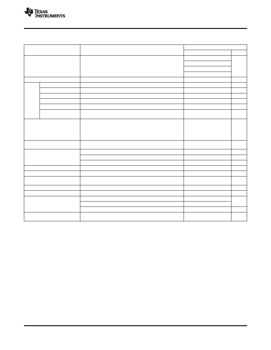
ELECTRICAL CHARACTERISTICS
operating at 25
°C free-air temperature, VI = 5 V, VO = 12 V, IO = IO (max), CI = 100 μF, CO = 100 μF (unless otherwise noted)
PARAMETER
TEST CONDITIONS
PTN04050C
MIN
TYP
MAX
UNIT
Over VI Range
VO = 15 V
0.1 (1)
0.8
VO = 12 V
0.1 (1)
1.0
IO
Output current
A
VO = 9 V
0.1 (1)
1.3
VO = 5 V
0.1 (1)
2.4
VI
Input voltage range
Over IO range
2.95
5.5 (2)
V
Output adjust range
5
15
V
Set-point voltage tolerance
TA = 25°C
±2 (3)
%VO
Temperature variation
–40°C to 85°C
±0.5
%VO
VO
Line regulation
Over VI range
±0.5
%VO
Load regulation
Over IO range
±0.5
%VO
Includes set point, line, load
Total Output Voltage
±3 (3)
%VO
Variation
–40°C < TA < 85°C
VI = 5 V, RSET = 60.4 , VO = 15 V
88%
VI = 5 V, RSET = 1.33 k, VO = 12 V
89%
η
Efficiency
VI = 5 V, RSET = 4.53 k, VO = 9 V
90%
VI = 3.3 V, RSET = OPEN, VO = 5 V
87%
Output voltage ripple
20-MHz bandwith
1.5
3
%VO
(peak-to-peak)
1 A/
μs load step from 50% to 100% IOmax
Transient response
Recovery time
500
μs
VO over/undershoot
2.5
%VO
Ilim
Current limit
150(4)
%IOmax
Iir
Inrush current
2(5)
A
Inrush current time
tir
1
ms
duration
FS
Switching frequency
Over VI and IO ranges
450
525
600
kHz
CI
External input capacitance
100 (6)
μF
Nonceramic
100 (7)
560 (8)
μF
External output
CO
Ceramic
0
100 (9)
capacitance
Equivalent series resistance (nonceramic)
10 (10)
m
Per Telcordia SR-332, 50% stress,
MTBF
Calculated reliability
8.9
106 Hr
TA = 40°C, ground benign
(1)
Operation at no load is not recommended.
(2)
The maximum VI is 5.5V or (VO- 0.5V) whichever is less. If the difference in VO to VIN is ≥ 0.5V and ≤ 1.4V, the device will operate in
asynchronous mode. In this condition, there may be multiple output voltage ripple frequencies and the total output voltage variation may
increase by up to 2%.
(3)
The set-point voltage tolerance is affected by the tolerance and stability of RSET. The stated limit is unconditionally met if RSET has a
tolerance of 1% with 100 ppm/
°C or better temperature stability.
(4)
Boost-topology switching regulators are not short-circuit protected.
(5)
The inrush current stated is in addition to the normal input current for the associated output load.
(6)
An external input capacitor is required across the input (VI and GND) for proper operation. See the application information for further
guidance.
(7)
An external output capacitance is required for proper operation. See the application information for further guidance.
(8)
The minimum ESR limitation may result in a lower value for the output capacitance. See the application information for further guidance.
(9)
When using ceramic capacitors equivalent to 100
μF, a 100 μF bulk electrolytic is also required.
(10) This is the minimum ESR for all the electrolytic (nonceramic) output capacitance. Use 17 m
as the minimum when using maximum
ESR values to calculate.
2005–2011, Texas Instruments Incorporated
3
Product Folder Link(s): PTN04050C
相关PDF资料 |
PDF描述 |
|---|---|
| PTN04050CAH | 1-OUTPUT 12 W DC-DC REG PWR SUPPLY MODULE |
| PTN78000AAST | 1-OUTPUT 9 W DC-DC REG PWR SUPPLY MODULE |
| PTN78000AAZ | 1-OUTPUT 9 W DC-DC REG PWR SUPPLY MODULE |
| PTN78000AAH | 1-OUTPUT 9 W DC-DC REG PWR SUPPLY MODULE |
| PTN78000HAST | 1-OUTPUT 22.5 W DC-DC REG PWR SUPPLY MODULE |
相关代理商/技术参数 |
参数描述 |
|---|---|
| PTN04050CAST | 功能描述:DC/DC转换器 12W 3.3/5V In Wide Adj Out Boost Cnvtr RoHS:否 制造商:Murata 产品: 输出功率: 输入电压范围:3.6 V to 5.5 V 输入电压(标称): 输出端数量:1 输出电压(通道 1):3.3 V 输出电流(通道 1):600 mA 输出电压(通道 2): 输出电流(通道 2): 安装风格:SMD/SMT 封装 / 箱体尺寸: |
| PTN04050CAZ | 功能描述:DC/DC转换器 12W 3.3/5V In Wide Adj Out Boost Cnvtr RoHS:否 制造商:Murata 产品: 输出功率: 输入电压范围:3.6 V to 5.5 V 输入电压(标称): 输出端数量:1 输出电压(通道 1):3.3 V 输出电流(通道 1):600 mA 输出电压(通道 2): 输出电流(通道 2): 安装风格:SMD/SMT 封装 / 箱体尺寸: |
| PTN04050CAZT | 功能描述:DC/DC转换器 12W 3.3/5V In Wide Adj Out Boost Cnvtr RoHS:否 制造商:Murata 产品: 输出功率: 输入电压范围:3.6 V to 5.5 V 输入电压(标称): 输出端数量:1 输出电压(通道 1):3.3 V 输出电流(通道 1):600 mA 输出电压(通道 2): 输出电流(通道 2): 安装风格:SMD/SMT 封装 / 箱体尺寸: |
| PTN0502E1000BBBS | 制造商:VISHAY 制造商全称:Vishay Siliconix 功能描述:Commercial Thin Film Chip Resistor, Surface Mount Chip |
| PTN0502E1000BBT3 | 制造商:VISHAY 制造商全称:Vishay Siliconix 功能描述:Commercial Thin Film Chip Resistor, Surface Mount Chip |
发布紧急采购,3分钟左右您将得到回复。