- 您现在的位置:买卖IC网 > PDF目录370028 > PXA250 (Intel Corp.) Intel-R PXA250 and PXA210 Applications Processors PDF资料下载
参数资料
| 型号: | PXA250 |
| 厂商: | Intel Corp. |
| 英文描述: | Intel-R PXA250 and PXA210 Applications Processors |
| 中文描述: | 英特尔- R的PXA250和PXA210应用处理器 |
| 文件页数: | 10/46页 |
| 文件大小: | 431K |
| 代理商: | PXA250 |
第1页第2页第3页第4页第5页第6页第7页第8页第9页当前第10页第11页第12页第13页第14页第15页第16页第17页第18页第19页第20页第21页第22页第23页第24页第25页第26页第27页第28页第29页第30页第31页第32页第33页第34页第35页第36页第37页第38页第39页第40页第41页第42页第43页第44页第45页第46页
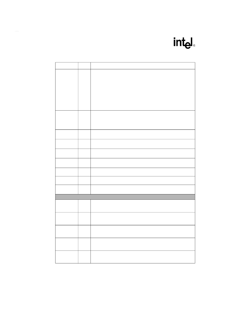
PXA250 and PXA210
—
Electrical, Mechanical, and Thermal Specification
10
Datasheet
SDCLK[2:0]
OCZ
SDRAM and/or Synchronous Static Memory clocks. Connect SDCLK[0] to the
clock (CLK) pins of SMROM and SDRAM-timing Synchronous Flash. SDCLK[1]
and SDCLK[2] should be connected to the clock pins of SDRAM in bank pairs 0/1
and 2/3, respectively. They are driven by either the internal memory controller
clock, or the internal memory controller clock divided by 2. At reset, all clock pins
are free running at the divide by 2 clock speed and may be turned off via free
running control register bits in the memory controller. The memory controller also
provides control register bits for clock division and deassertion of each SDCLK
pin. SDCLK[0] control register assertion bit defaults to on if the boot-time static
memory bank 0 is configured for SMROM or SDRAM-timing Synchronous Flash.
SDCLK[2:1] control register assertion bits are always deasserted upon reset.
0 and 2 are not three-stateable, SDCLK1 is three-stateable
nCS[5]/
GPIO[33]
ICOCZ
Static chip selects. These signals are chip selects for static memory devices such
as ROM and Flash. They are individually programmable in the memory
configuration registers. nCS[5:3] may be used with variable data latency variable
latency I/O devices.
See Note [1]
nCS[4]/
GPIO[80]
ICOCZ
Static chip select 4.
nCS[3]/
GPIO[79]
ICOCZ
Static chip select 3.
nCS[2]/
GPIO[78]
ICOCZ
Static chip select 2.
nCS[1]/
GPIO[15]
ICOCZ
Static chip select 1.
nCS[0]
ICOCZ
Static chip select 0. This is the boot memory chip select. nCS[0] is a dedicated
pin.
RD/nWR
OCZ
Read/Write for static interface. Intended for use as a steering signal for buffering
logic
RDY/
GPIO[18]
ICOCZ
Variable Latency I/O Ready pin (input)
See Note [1]
PCMCIA/CF Control Pins
nPOE/
GPIO[48]
ICOCZ
PCMCIA Output Enable. This PCMCIA signal is an output and performs reads
from memory and attribute space.
See Note [1]
nPWE/
GPIO[49]
ICOCZ
PCMCIA Write Enable. This signal is an output and performs writes to memory
and attribute space.
See Note [1]
nPIOW/
GPIO[51]
ICOCZ
PCMCIA I/O Write. This signal is an output and performs write transactions to the
PCMCIA I/O space.
See Note [1]
nPIOR/
GPIO[50]
ICOCZ
PCMCIA I/O Read. This signal is an output and performs read transactions from
the PCMCIA I/O space.
See Note [1]
nPCE[2:1]/
GPIO[53, 52]
ICOCZ
PCMCIA Card Enable. These signals are outputs and select a PCMCIA card. Bit
one enables the high byte lane and bit zero enables the low byte lane.
See Note [1]
Table 2. Pin and Signal Descriptions for the PXA250 Applications Processor (Sheet 2 of 7)
Name
Type
Description
相关PDF资料 |
PDF描述 |
|---|---|
| PXA255 | PXA255 Processor |
| PXA270 | Electrical, Mechanical, and Thermal Specification |
| PXAC37 | XA 16-bit microcontroller family 32K/1024 OTP CAN transport layer controller 1 UART, 1 SPI Port, CAN 2.0B, 32 CAN ID Filters, transport layer co-proce |
| PXB16050U | NPN microwave power transistor |
| PY08-02 | INDUSTRIERELAIS FASSUNG PCB |
相关代理商/技术参数 |
参数描述 |
|---|---|
| PXA250B2C400 | 制造商:Intel 功能描述:Microprocessor, 32 Bit, 256 Pin, Plastic, BGA |
| PXA250C0C400 | 制造商:Intel 功能描述:IC,MICROPROCESSOR,32-BIT,CMOS,BGA,256PIN,PLASTIC |
| PXA255 | 制造商:INTEL 制造商全称:Intel Corporation 功能描述:PXA255 Processor |
| PXA25VC22RMH70TP | 制造商:United Chemi-Con Inc 功能描述:Cap Aluminum 22uF 25V 20% (8 X 6.7mm) SMD 0.05 Ohm 1800mA 2000 hr 105°C T/R |
| PXA270 | 制造商:INTEL 制造商全称:Intel Corporation 功能描述:Electrical, Mechanical, and Thermal Specification |
发布紧急采购,3分钟左右您将得到回复。