- 您现在的位置:买卖IC网 > PDF目录368401 > PZ5032NS7A44 Electrically-Erasable Complex PLD PDF资料下载
参数资料
| 型号: | PZ5032NS7A44 |
| 英文描述: | Electrically-Erasable Complex PLD |
| 中文描述: | 电可擦除复杂可编程逻辑器件 |
| 文件页数: | 9/14页 |
| 文件大小: | 107K |
| 代理商: | PZ5032NS7A44 |
Philips Semiconductors
Product specification
PZ5032
32 macrocell CPLD
1997 Feb 20
9
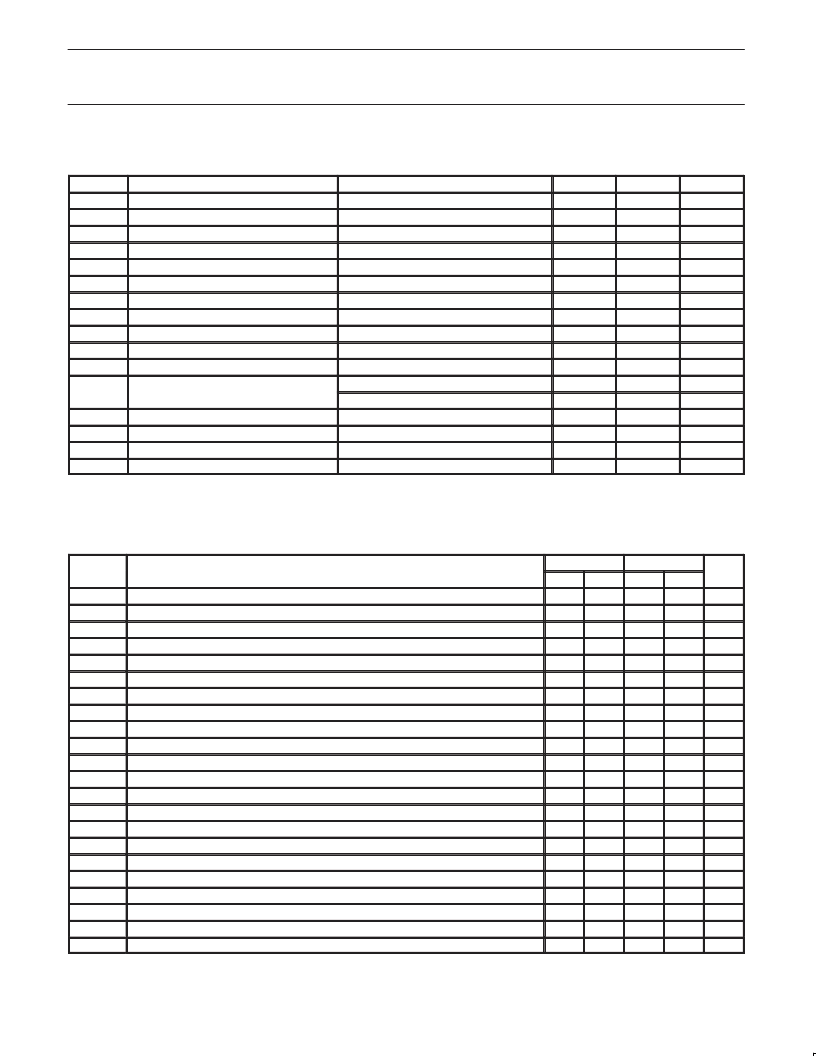
DC ELECTRICAL CHARACTERISTICS FOR INDUSTRIAL GRADE DEVICES
Industrial:
–40
°
C
≤
T
amb
≤
+85
°
C; 4.5V
≤
V
DD
≤
5.5V
SYMBOL
PARAMETER
V
IL
Input voltage low
V
IH
Input voltage high
V
I
Input clamp voltage
V
OL
Output voltage low
V
OH
Output voltage high
I
IL
Input leakage current low
I
IH
Input leakage current high
I
IL
Clock input leakage current
I
OZL
3-Stated output leakage current low
I
OZH
3-Stated output leakage current high
I
DDQ
Standby current
TEST CONDITIONS
V
DD
= 4.5V
V
DD
= 5.5V
V
DD
= 4.5V, I
IN
= –18mA
V
DD
= 4.5V, I
OL
= 12mA
V
DD
= 4.5V, I
OH
= –12mA
V
DD
= 5.5V (except CKO), V
IN
= 0.4V
V
DD
= 5.5V, V
IN
= 3.0V
V
DD
= 5.5V, V
IN
= 0.4V
V
DD
= 5.5V, V
IN
= 0.4V
V
DD
= 5.5V, V
IN
= 3.0V
V
DD
= 5.5V, T
amb
= –40
°
C
V
DD
= 5.5V, T
amb
= –40
°
C @ 1MHz
V
DD
= 5.5V, T
amb
= –40
°
C @ 50MHz
1 pin at a time for no longer than 1 second
T
amb
= 25
°
C, f = 1MHz
T
amb
= 25
°
C, f = 1MHz
T
amb
= 25
°
C, f = 1MHz
MIN.
MAX.
0.8
UNIT
V
V
V
V
V
μ
A
μ
A
μ
A
μ
A
μ
A
μ
A
mA
mA
mA
pF
pF
pF
2.0
–1.2
0.5
2.4
–10
–10
–10
–10
–10
10
10
10
10
10
95
4
35
–230
8
12
10
I
DDD1
Dynamic current
I
OS
C
IN
C
CLK
C
I/O
Short circuit output current
Input pin capacitance
Clock input capacitance
I/O pin capacitance
–50
5
NOTE:
1. This parameter measured with a 16–bit, loadable up/down counter loaded into every logic block, with all outputs enabled and unloaded.
Inputs are tied to V
DD
or ground. This parameter guaranteed by design and characterization, not testing.
AC ELECTRICAL CHARACTERISTICS
1
FOR INDUSTRIAL GRADE DEVICES
Industrial:
–40
°
C
≤
T
amb
≤
+85
°
C; 4.5V
≤
V
DD
≤
5.5V
SYMBOL
PARAMETER
I7
I10
UNIT
MIN.
2
3
2
5
7
MAX.
7.5
9.5
6
MIN.
2
3
2
8
10.5
MAX.
10
12.5
9
t
PD_PAL
t
PD_PLA
t
CO
t
SU_PAL
t
SU_PLA
t
H
t
CH
t
CL
t
R
t
F
f
MAX1
f
MAX2
f
MAX3
t
BUF
t
PDF_PAL
t
PDF_PLA
t
CF
t
INIT
t
ER
t
EA
t
RP
t
RR
NOTES:
1. Specifications measured with one output switching. See Figure 6 and Table 3 for derating.
2. This parameter guaranteed by design and characterization, not by test.
3. Output C
L
= 5pF.
Propagation delay time, input (or feedback node) to output through PAL
Propagation delay time, input (or feedback node) to output through PAL & PLA
Clock to out delay time
Setup time (from input or feedback node) through PAL
Setup time (from input or feedback node) through PAL + PLA
Hold time
Clock High time
Clock Low time
Input rise time
Input fall time
Maximum FF toggle rate
2
(1/t
CH
+ t
CL
)
Maximum internal frequency
2
(1/t
SUPAL
+ t
CF
)
Maximum external frequency
2
(1/t
SUPAL
+ t
CO
)
Output buffer delay time
Input (or feedback node) to internal feedback node delay time through PAL
Input (or feedback node) to internal feedback node delay time through PAL + PLA
Clock to internal feedback node delay time
Delay from valid V
DD
to valid reset
Input to output disable
3
Input to output valid
Input to register preset
Input to register reset
ns
ns
ns
ns
ns
ns
ns
ns
ns
ns
MHz
MHz
MHz
ns
ns
ns
ns
μ
s
ns
ns
ns
ns
0
0
4
4
5
5
20
20
20
20
125
105
91
100
64
59
1.5
6
8
4.5
50
12
12
12
14
1.5
8.5
11
7.5
50
15
15
15
18
相关PDF资料 |
PDF描述 |
|---|---|
| PZ5032NS7BC | Electrically-Erasable Complex PLD |
| PZ5032NS7BC-S | Electrically-Erasable Complex PLD |
| PZ5032CS10BC | Electrically-Erasable Complex PLD |
| PZ5032CS10BC-S | Electrically-Erasable Complex PLD |
| PZ5032CS6A44 | Electrically-Erasable Complex PLD |
相关代理商/技术参数 |
参数描述 |
|---|---|
| PZ5128-S7BP | 制造商: 功能描述: 制造商:undefined 功能描述: |
| PZ-5-3 | 制造商:WM BERG 功能描述: |
| PZ5CG | 制造商:未知厂家 制造商全称:未知厂家 功能描述:0.5 KV ISOLATED 0.75 W REGULATED SINGLE OUTPUT SIP7 |
| PZ5CG-0505E | 制造商:未知厂家 制造商全称:未知厂家 功能描述:0.5 KV ISOLATED 0.75 W REGULATED SINGLE OUTPUT SIP7 |
| PZ5CG-0512E | 制造商:未知厂家 制造商全称:未知厂家 功能描述:0.5 KV ISOLATED 0.75 W REGULATED SINGLE OUTPUT SIP7 |
发布紧急采购,3分钟左右您将得到回复。