- 您现在的位置:买卖IC网 > PDF目录296939 > QL4016-2PF144M (QUICKLOGIC CORP) FPGA, 320 CLBS, 61280 GATES, PQFP144 PDF资料下载
参数资料
| 型号: | QL4016-2PF144M |
| 厂商: | QUICKLOGIC CORP |
| 元件分类: | FPGA |
| 英文描述: | FPGA, 320 CLBS, 61280 GATES, PQFP144 |
| 封装: | 20 X 20 MM, 1.40 MM HEIGHT, TQFP-144 |
| 文件页数: | 3/45页 |
| 文件大小: | 1332K |
| 代理商: | QL4016-2PF144M |
第1页第2页当前第3页第4页第5页第6页第7页第8页第9页第10页第11页第12页第13页第14页第15页第16页第17页第18页第19页第20页第21页第22页第23页第24页第25页第26页第27页第28页第29页第30页第31页第32页第33页第34页第35页第36页第37页第38页第39页第40页第41页第42页第43页第44页第45页
2007 QuickLogic Corporation
QuickRAM Family Data Sheet Rev. M
11
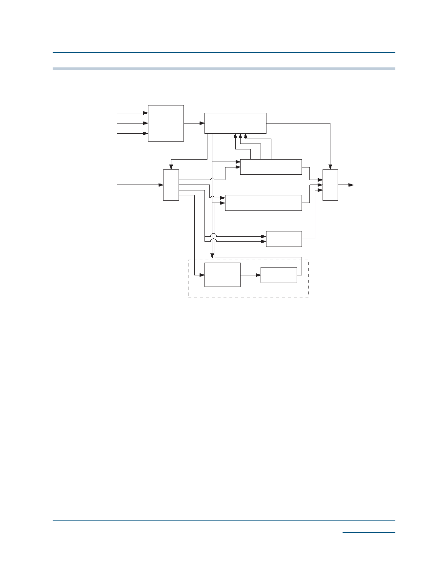
JTAG
Figure 9: JTAG Block Diagram
Microprocessors and Application Specific Integrated Circuits (ASICs) pose many design challenges, not the
least of which concerns the accessibility of test points. The Joint Test Access Group (JTAG) formed in response
to this challenge, resulting in IEEE standard 1149.1, the Standard Test Access Port and Boundary Scan
Architecture.
The JTAG boundary scan test methodology allows complete observation and control of the boundary pins of
a JTAG-compatible device through JTAG software. A Test Access Port (TAP) controller works in concert with
the Instruction Register (IR); these allow users to run three required tests, along with several user-defined tests.
JTAG tests allow users to reduce system debug time, reuse test platforms and tools, and reuse subsystem tests
for fuller verification of higher level system elements.
The 1149.1 standard requires the following three tests:
Extest Instruction. The Extest Instruction performs a Printed Circuit Board (PCB) interconnect test. This
test places a device into an external boundary test mode, selecting the boundary scan register to be
connected between the TAP Test Data In (TDI) and Test Data Out (TDO) pins. Boundary scan cells are
preloaded with test patterns (via the Sample/Preload Instruction), and input boundary cells capture the input
data for analysis.
Sample/Preload Instruction. The Sample/Preload Instruction allows a device to remain in its functional
mode, while selecting the boundary scan register to be connected between the TDI and TDO pins. For this
test, the boundary scan register can be accessed via a data scan operation, allowing users to sample the
functional data entering and leaving the device.
TCK
TMS
TRSTB
RDI
TDO
Instruction Decode
and
Control Logic
TAP Controller
State Machine
(16 States)
Instruction Register
Boundary-ScanRegister
(Data Register)
Mux
Bypass
Register
Mux
Internal
Register
I/O Registers
User Defined Data Register
相关PDF资料 |
PDF描述 |
|---|---|
| QL4016-0PF84C | FPGA, 320 CLBS, 61280 GATES, PQCC84 |
| QL4016-0PF84I | FPGA, 320 CLBS, 61280 GATES, PQCC84 |
| QL4016-1PF84C | FPGA, 320 CLBS, 61280 GATES, PQCC84 |
| QL4016-1PF84I | FPGA, 320 CLBS, 61280 GATES, PQCC84 |
| QL4016-2PF84C | FPGA, 320 CLBS, 61280 GATES, PQCC84 |
相关代理商/技术参数 |
参数描述 |
|---|---|
| QL4016-2PFN144C-6107 | 制造商:QuickLogic Corporation 功能描述: |
| QL4016-2PG208M | 制造商:未知厂家 制造商全称:未知厂家 功能描述:90,000 Usable PLD Gate QuickRAM Combining Performance, Density and Embedded RAM |
| QL4016-2PG208M/883 | 制造商:未知厂家 制造商全称:未知厂家 功能描述:90,000 Usable PLD Gate QuickRAM Combining Performance, Density and Embedded RAM |
| QL4016-2PL84C | 制造商:未知厂家 制造商全称:未知厂家 功能描述:16,000 Usable PLD Gate QuickRAM ESP Combining Performance, Density and Embedded RAM |
| QL4016-2PL84I | 制造商:未知厂家 制造商全称:未知厂家 功能描述:16,000 Usable PLD Gate QuickRAM ESP Combining Performance, Density and Embedded RAM |
发布紧急采购,3分钟左右您将得到回复。