- 您现在的位置:买卖IC网 > PDF目录296939 > QL4016-3PF84I (QUICKLOGIC CORP) FPGA, 320 CLBS, 61280 GATES, PQCC84 PDF资料下载
参数资料
| 型号: | QL4016-3PF84I |
| 厂商: | QUICKLOGIC CORP |
| 元件分类: | FPGA |
| 英文描述: | FPGA, 320 CLBS, 61280 GATES, PQCC84 |
| 封装: | PLASTIC, LCC-84 |
| 文件页数: | 4/45页 |
| 文件大小: | 1332K |
| 代理商: | QL4016-3PF84I |
第1页第2页第3页当前第4页第5页第6页第7页第8页第9页第10页第11页第12页第13页第14页第15页第16页第17页第18页第19页第20页第21页第22页第23页第24页第25页第26页第27页第28页第29页第30页第31页第32页第33页第34页第35页第36页第37页第38页第39页第40页第41页第42页第43页第44页第45页
2007 QuickLogic Corporation
QuickRAM Family Data Sheet Rev. M
12
Bypass Instruction. The Bypass Instruction allows data to skip a device boundary scan entirely, so the
data passes through the bypass register. The Bypass instruction allows users to test a device without passing
through other devices. The bypass register is connected between the TDI and TDO pins, allowing serial data
to be transferred through a device without affecting the operation of the device.
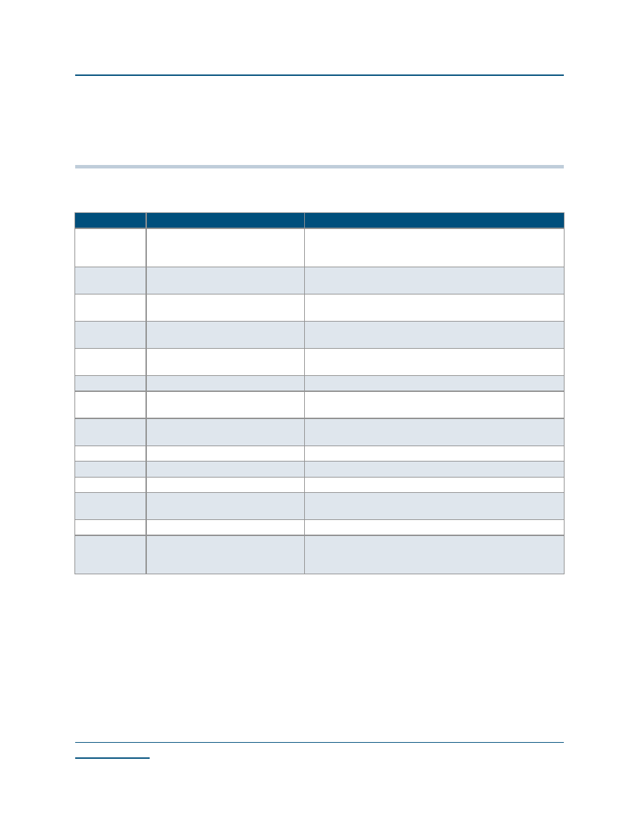
Pin Descriptions
Table 14: Pin Descriptions
Pin
Function
Description
TDI/RSI
Test Data In for JTAG /RAM init.
Serial Data In
Hold HIGH during normal operation. Connects to serial
PROM data in for RAM initialization. Connect to VCC if
unused.
TRSTB/RRO
Active low Reset for JTAG /RAM init.
reset out
Hold LOW during normal operation. Connects to serial PROM
reset for RAM initialization. Connect to GND if unused.
TMS
Test Mode Select for JTAG
Hold HIGH during normal operation. Connect to VCC if not
used for JTAG.
TCK
Test Clock for JTAG
Hold HIGH or LOW during normal operation. Connect to VCC
or ground if not used for JTAG.
TDO/RCO
Test data out for JTAG /RAM init.
clock out
Connect to serial PROM clock for RAM initialization. Must be
left unconnected if not used for JTAG or RAM initialization.
STM
Special Test Mode
Must be grounded during normal operation.
I/ACLK
High-drive input and/or array
network driver
Can be configured as either or both.
I/GCLK
High-drive input and/or global
network driver
Can be configured as either or both.
I
High-drive input
Use for input signals with high fanout.
I/O
Input/Output pin
Can be configured as an input and/or output.
V
CC
Power supply pin
Connect to 3.3 V supply.
VCCIO
Input voltage tolerance pin
Connect to 5.0 V supply if 5 V input tolerance is required,
otherwise connect to 3.3 V supply.
GND
Ground pin
Connect to ground.
GND/THERM
Ground/Thermal pin
Available on 456-PBGA only. Connect to ground plane on
PCB if heat sinking desired. Otherwise may be left
unconnected.
相关PDF资料 |
PDF描述 |
|---|---|
| QL4016-3PF84M | FPGA, 320 CLBS, 61280 GATES, PQCC84 |
| QL4016-3PFN100M | FPGA, 320 CLBS, 61280 GATES, PQFP100 |
| QL4016-3PFN144M | FPGA, 320 CLBS, 61280 GATES, PQFP144 |
| QL4016-4CF100M | FPGA, 320 CLBS, 61280 GATES, CQFP100 |
| QL4016-4PF100M | FPGA, 320 CLBS, 61280 GATES, PQFP100 |
相关代理商/技术参数 |
参数描述 |
|---|---|
| QL4016-3PL84C | 制造商:未知厂家 制造商全称:未知厂家 功能描述:16,000 Usable PLD Gate QuickRAM ESP Combining Performance, Density and Embedded RAM |
| QL4016-3PL84I | 制造商:未知厂家 制造商全称:未知厂家 功能描述:16,000 Usable PLD Gate QuickRAM ESP Combining Performance, Density and Embedded RAM |
| QL4016-3PL84M | 制造商:未知厂家 制造商全称:未知厂家 功能描述:16,000 Usable PLD Gate QuickRAM ESP Combining Performance, Density and Embedded RAM |
| QL4016-3PLC | 制造商:未知厂家 制造商全称:未知厂家 功能描述:16,000 Usable PLD Gate QuickRAM ESP Combining Performance, Density and Embedded RAM |
| QL4016-3PLI | 制造商:未知厂家 制造商全称:未知厂家 功能描述:16,000 Usable PLD Gate QuickRAM ESP Combining Performance, Density and Embedded RAM |
发布紧急采购,3分钟左右您将得到回复。