- 您现在的位置:买卖IC网 > PDF目录361292 > QL6250PS484 ASIC PDF资料下载
参数资料
| 型号: | QL6250PS484 |
| 英文描述: | ASIC |
| 中文描述: | 专用集成电路 |
| 文件页数: | 1/13页 |
| 文件大小: | 165K |
| 代理商: | QL6250PS484 |
Eclipse
TM
Family Data Sheet
1
Eclipse Family Data Sheet
Combining Performance, Density and Embedded RAM
1.0 Device Highlights
Flexible Programmable Logic
.25u, 5 layer metal CMOS process
2.5 V Vcc, 2.5/3.3 V drive capable I/O
Up to 4032 SuperCells
Up to 583,000 Max System Gates
Up to 512 I/O
Embedded Dual Port SRAM
Up to 36-2,304 bit Dual Port High
performance SRAM Blocks
Up to 82,900 RAM bits
RAM/ROM/FIFO Wizard for automatic
configuration
Configurable and Cascadable
Applications
Signal processing operators
Signal processing functions
Networking / communications for VoIP
Speech / voice processing
Channel coding
Programmable I/O
High performance Enhanced I/O (EIO):
Less than 3 ns Tco
Programmable Slew Rate Control
Programmable I/O Standards
LVTTL, LVCMOS, PCI, GTL+, SSTL2,
and SSTL3
8 Independent I/O Banks
3 Register Configuration: Input, Output, OE
Advanced Clock Network
9 Global Clock Networks
1 dedicated
8 programmable
16 I/O (high drive) Networks:
2 I/O’s per bank
20 Quad-Net Networks: 5 per quadrant
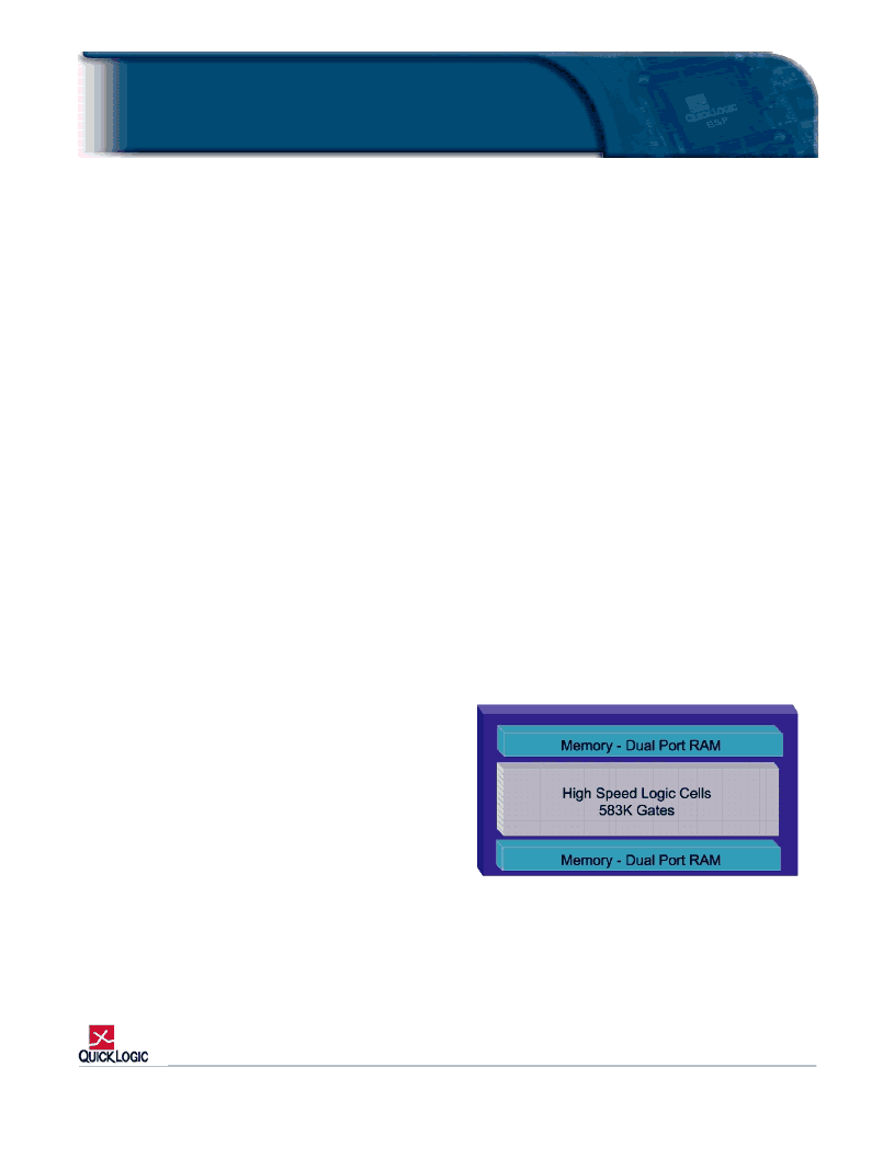
Figure 1: Embedded Eclipse Block Diagram
相关PDF资料 |
PDF描述 |
|---|---|
| QL6250PS672 | ASIC |
| QL6250PT280 | ASIC |
| QL6325PQ208 | ASIC |
| QL6325PT280 | ASIC |
| QL6500PB516 | Power choke, toroid, RoHS |
相关代理商/技术参数 |
参数描述 |
|---|---|
| QL6325PQ208 | 制造商:未知厂家 制造商全称:未知厂家 功能描述:ASIC |
| QL6325PT280 | 制造商:未知厂家 制造商全称:未知厂家 功能描述:ASIC |
| QL63D5SA | 制造商:未知厂家 制造商全称:未知厂家 功能描述:InGaAlP Laser Diode |
| QL63F5SA | 制造商:未知厂家 制造商全称:未知厂家 功能描述:InGaAlP Laser Diode |
| QL63H5S-A | 制造商:ROITHNER 制造商全称:ROITHNER 功能描述:INGaAIP Laser Diode |
发布紧急采购,3分钟左右您将得到回复。