- 您现在的位置:买卖IC网 > PDF目录296941 > QL8150-7PFN144C (QUICKLOGIC CORP) FPGA, 640 CLBS, 188946 GATES, PQFP144 PDF资料下载
参数资料
| 型号: | QL8150-7PFN144C |
| 厂商: | QUICKLOGIC CORP |
| 元件分类: | FPGA |
| 英文描述: | FPGA, 640 CLBS, 188946 GATES, PQFP144 |
| 封装: | LEAD FREE, TQFP-144 |
| 文件页数: | 2/96页 |
| 文件大小: | 1607K |
| 代理商: | QL8150-7PFN144C |
第1页当前第2页第3页第4页第5页第6页第7页第8页第9页第10页第11页第12页第13页第14页第15页第16页第17页第18页第19页第20页第21页第22页第23页第24页第25页第26页第27页第28页第29页第30页第31页第32页第33页第34页第35页第36页第37页第38页第39页第40页第41页第42页第43页第44页第45页第46页第47页第48页第49页第50页第51页第52页第53页第54页第55页第56页第57页第58页第59页第60页第61页第62页第63页第64页第65页第66页第67页第68页第69页第70页第71页第72页第73页第74页第75页第76页第77页第78页第79页第80页第81页第82页第83页第84页第85页第86页第87页第88页第89页第90页第91页第92页第93页第94页第95页第96页
2007 QuickLogic Corporation
Eclipse II Family Data Sheet Rev. Q
10
become a greater issue with specific requirements for setup, hold, clock to out, and switching times. Eclipse II
has addressed these new system requirements and now includes a completely new I/O cell which consists of
programmable I/Os as well as a new cell structure consisting of three registers—Input, Output, and OE.
Eclipse II offers banks of programmable I/Os that address many of the bus standards that are popular today.
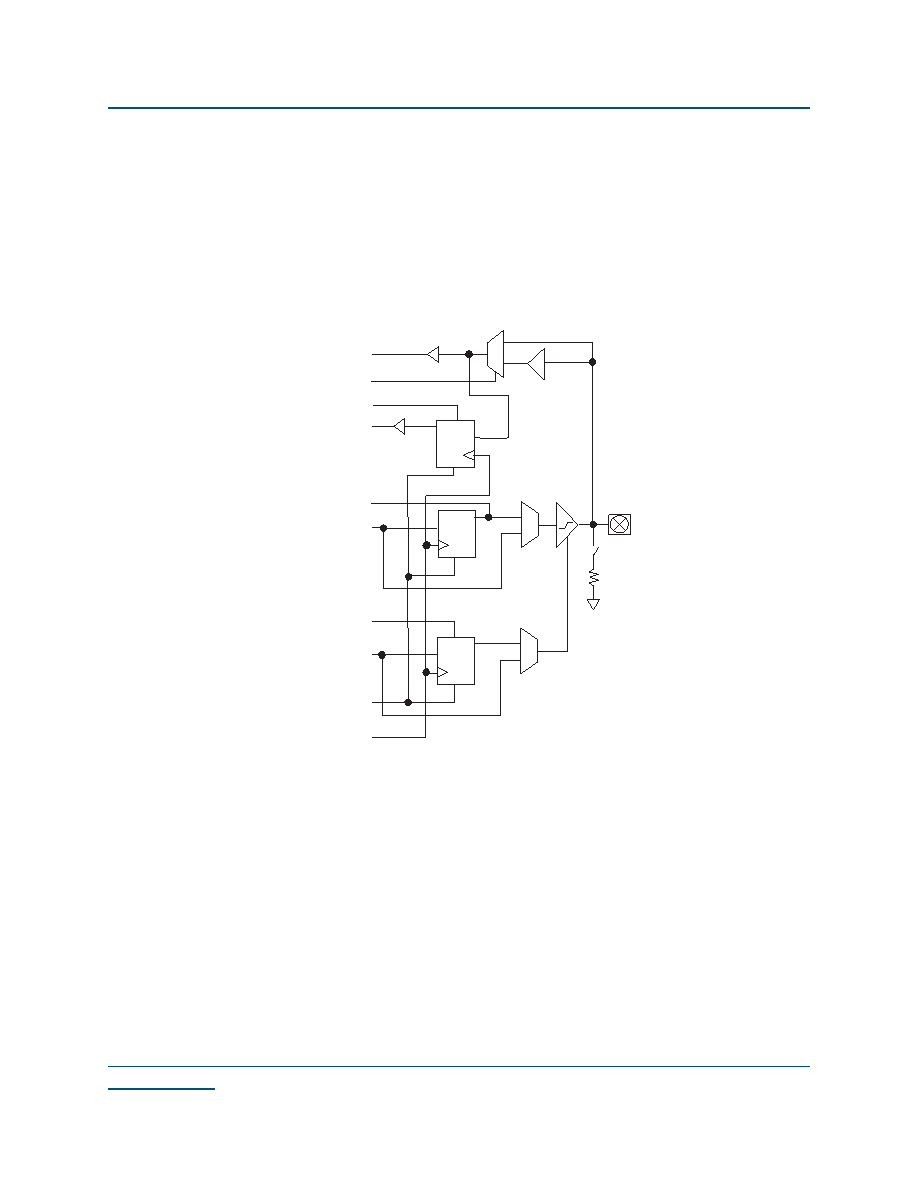
As shown in Figure 7 each bi-directional I/O pin is associated with an I/O cell which features an input register,
an input buffer, an output register, a three-state output buffer, an output enable register, and 2 two-to-one
output multiplexers.
Figure 7: Eclipse II I/O Cell
The bi-directional I/O pin options can be programmed for input, output, or bi-directional operation. As shown
in Figure 7, each bi-directional I/O pin is associated with an I/O cell which features an input register, an input
buffer, an output register, a three-state output buffer, an output enable register, and 2 two-to-one multiplexers.
The select lines of the two-to-one multiplexers are static and must be connected to either VCC or GND.
For input functions, I/O pins can provide combinatorial, registered data, or both options simultaneously to the
logic array. For combinatorial input operation, data is routed from I/O pins through the input buffer to the
array logic. For registered input operation, I/O pins drive the D input of input cell registers, allowing data to
be captured with fast, predictable set-up times without consuming internal logic cell resources. The comparator
and multiplexer in the input path allows for native support of I/O standards with reference points offset from
traditional ground.
For output functions, I/O pins can receive combinatorial or registered data from the logic array. For
combinatorial output operation, data is routed from the logic array through a multiplexer to the I/O pin. For
registered output operation, the array logic drives the D input of the output cell register which in turn drives
the I/O pin through a multiplexer. The multiplexer allows either a combinatorial or a registered signal to be
E
R
Q
D
R
Q
D
E
R
Q
D
+
-
PAD
OUTPUT ENABLE
REGISTER
OUTPUT
REGISTER
INPUT
REGISTER
相关PDF资料 |
PDF描述 |
|---|---|
| QL8150-7PFN144I | FPGA, 640 CLBS, 188946 GATES, PQFP144 |
| QL8150-7PFN144M | FPGA, 640 CLBS, 188946 GATES, PQFP144 |
| QL8150-8PFN144C | FPGA, 640 CLBS, 188946 GATES, PQFP144 |
| QL8150-8PFN144I | FPGA, 640 CLBS, 188946 GATES, PQFP144 |
| QL8150-8PTN196M | FPGA, 640 CLBS, 188946 GATES, PBGA196 |
相关代理商/技术参数 |
参数描述 |
|---|---|
| QL8250 | 制造商:未知厂家 制造商全称:未知厂家 功能描述:LOW POWER FPGA COMBINING PERFORMANCE DENSITY AND EMBEDED RAM |
| QL8250-6PQN208C-5690 | 制造商:QuickLogic Corporation 功能描述: |
| QL8250-6PQN208C-5691 | 制造商:QuickLogic Corporation 功能描述: |
| QL82SD | 制造商:未知厂家 制造商全称:未知厂家 功能描述:10 High Speed Bus LVDS Serial Links bandwidth up to 5 Gbps |
| QL82SD-PB516 | 制造商:未知厂家 制造商全称:未知厂家 功能描述:10 High Speed Bus LVDS Serial Links bandwidth up to 5 Gbps |
发布紧急采购,3分钟左右您将得到回复。