参数资料
| 型号: | QLX4600SIQSR |
| 厂商: | Intersil |
| 文件页数: | 17/23页 |
| 文件大小: | 0K |
| 描述: | IC EQUALIZER REC 6.25GBPS 46QFN |
| 标准包装: | 100 |
| 系列: | QLx™ |
| 应用: | 铜电缆模块 |
| 电源电压: | 1.1 V ~ 1.3 V |
| 封装/外壳: | 46-WFQFN 裸露焊盘 |
| 供应商设备封装: | 46-TQFN |
| 包装: | 带卷 (TR) |
| 安装类型: | 表面贴装 |
3
FN6979.1
November 19, 2009
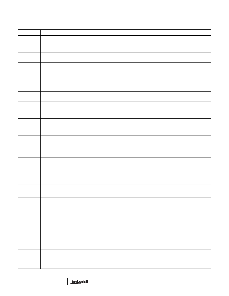
Pin Descriptions
PIN NAME
PIN NUMBER
DESCRIPTION
DT
1
Detection Threshold. Reference DC CURRENT threshold for input signal power detection. Data
output Out[k] is muted when the power of the equalized version of In[k] falls below the
threshold. Tie to ground to disable electrical idle preservation and always enable the limiting
amplifier.
IN1[P,N]
2, 3
Equalizer 1 differential input, CML. The use of 100nF low ESL/ESR MLCC capacitor with at least
4GHz frequency response is recommended.
VDD
4, 7, 10, 29,
32, 35
Power supply. 1.2V supply voltage. The use of parallel 100pF and 10nF decoupling capacitors to
ground is recommended for each of these pins for broad high-frequency noise suppression.
IN2[P,N]
5, 6
Equalizer 2 differential input, CML. The use of 100nF low ESL/ESR MLCC capacitor with at least
4GHz frequency response is recommended.
IN3[P,N]
8, 9
Equalizer 3 differential input, CML. The use of 100nF low ESL/ESR MLCC capacitor with at least
4GHz frequency response is recommended.
IN4[P,N]
11, 12
Equalizer 4 differential input, CML. The use of 100nF low ESL/ESR MLCC capacitor with at least
4GHz frequency response is recommended.
IS1
13
Impedance Select 1. CMOS logic input. When the voltage on this pin is LOW, the single-ended
input impedance of In1P and In1N each go above 200kΩ and powers down the channel. This pin
should be connected to the Fundamental Reset signal in PCI Express. Otherwise, connect to
VDD to hold the input impedance at 50Ω.
IS2
14
Impedance Select 2. CMOS logic input. When the voltage on this pin is LOW, the single-ended
input impedance of In2P and In2N each go above 200kΩ and powers down the channel. This pin
should be connected to the Fundamental Reset signal in PCI Express. Otherwise, connect to
VDD to hold the input impedance at 50Ω.
GND
15
Ground
DI
16
Serial data input, CMOS logic. Input for serial data stream to program internal registers
controlling the boost for all four equalizers. Synchronized with clock (CLK) on pin 46. Overrides
the boost setting established on CP control pins. Internally pulled down.
DO
17
Serial data output, CMOS logic. Output of the internal registers controlling the boost for all four
equalizers. Synchronized with clock on pin 46. Equivalent to serial data input on DI but delayed
by 21 clock cycles.
CP3[A,B,C]
18, 19, 20
Control pins for setting equalizer 3. CMOS logic inputs. Pins are read as a 3-digit number to set
the boost level. A is the MSB, and C is the LSB. Pins are internally pulled down through a 25kΩ
resistor.
CP4[A,B,C]
21, 22, 23
Control pins for setting equalizer 4. CMOS logic inputs. Pins are read as a 3-digit number to set
the boost level. A is the MSB, and C is the LSB. Pins are internally pulled down through a 25kΩ
resistor.
MODE
24
Boost-level control mode input, CMOS logic. Allows serial programming of internal registers
through pins DI, ENB, and Clk when set HIGH. Resets all internal registers to zero and uses boost
levels set by CP pins when set LOW. If serial programming is not used, this pin should be
grounded.
IS4
25
Impedance Select 4. CMOS logic input. When the voltage on this pin is LOW, the single-ended
input impedance of In4P and In4N each go above 200kΩ and powers down the channel. This pin
should be connected to the Fundamental Reset signal in PCI Express. Otherwise, connect to
VDD to hold the input impedance at 50Ω.
IS3
26
Impedance Select 3. CMOS logic input. When the voltage on this pin is LOW, the single-ended
input impedance of In3P and In3N each go above 200kΩ and powers down the channel. This pin
should be connected to the Fundamental Reset signal in PCI Express. Otherwise, connect to
VDD to hold the input impedance at 50Ω.
OUT4[N,P]
27, 28
Equalizer 4 differential output, CML. The use of 100nF low ESL/ESR MLCC capacitor with at least
4GHz frequency response is recommended.
OUT3[N,P]
30, 31
Equalizer 3 differential output, CML. The use of 100nF low ESL/ESR MLCC capacitor with at least
4GHz frequency response is recommended.
QLx4600-S30
相关PDF资料 |
PDF描述 |
|---|---|
| R5F100GEAFB#V0 | MCU 16BIT 64KB FLASH 48LQFP |
| R5F2135CMNFP#V0 | IC MICROCONTROLLER |
| R5F562N8ADBG#U0 | MCU 32BIT FLASH 512KROM 176LFBGA |
| R5F5630ADDFB#V0 | MCU RX630 768KB FLASH 144-LQFP |
| R5F72167GDFA#V0 | MCU 1MB FLASH 128K 176-LQFP |
相关代理商/技术参数 |
参数描述 |
|---|---|
| QLX4600SIQT7 | 功能描述:接口 - 专用 6 GBS QD CH LANE EXTENDER RoHS:否 制造商:Texas Instruments 产品类型:1080p60 Image Sensor Receiver 工作电源电压:1.8 V 电源电流:89 mA 最大功率耗散: 最大工作温度:+ 85 C 安装风格:SMD/SMT 封装 / 箱体:BGA-59 |
| QLX4600-SL30 | 制造商:INTERSIL 制造商全称:Intersil Corporation 功能描述:Quad Lane Extender |
| QLZ06 0012-2513 | 制造商:ebm-papst Inc 功能描述: |
| QLZ06 0018-2518 | 制造商:ebm-papst Inc 功能描述: |
| QLZ06 0600-2513 | 制造商:Ebm-Papst Industries 功能描述:Bulk |
发布紧急采购,3分钟左右您将得到回复。