- 您现在的位置:买卖IC网 > PDF目录269903 > QS74FCT2823ATQ (INTEGRATED DEVICE TECHNOLOGY INC) FCT SERIES, 9-BIT DRIVER, TRUE OUTPUT, PDSO24 PDF资料下载
参数资料
| 型号: | QS74FCT2823ATQ |
| 厂商: | INTEGRATED DEVICE TECHNOLOGY INC |
| 元件分类: | 总线收发器 |
| 英文描述: | FCT SERIES, 9-BIT DRIVER, TRUE OUTPUT, PDSO24 |
| 封装: | QSOP-24 |
| 文件页数: | 2/7页 |
| 文件大小: | 60K |
| 代理商: | QS74FCT2823ATQ |
2
INDUSTRIALTEMPERATURERANGE
IDTQS74FCT2823AT/BT
HIGH-SPEEDCMOSBUSINTERFACE9-BITREGISTER
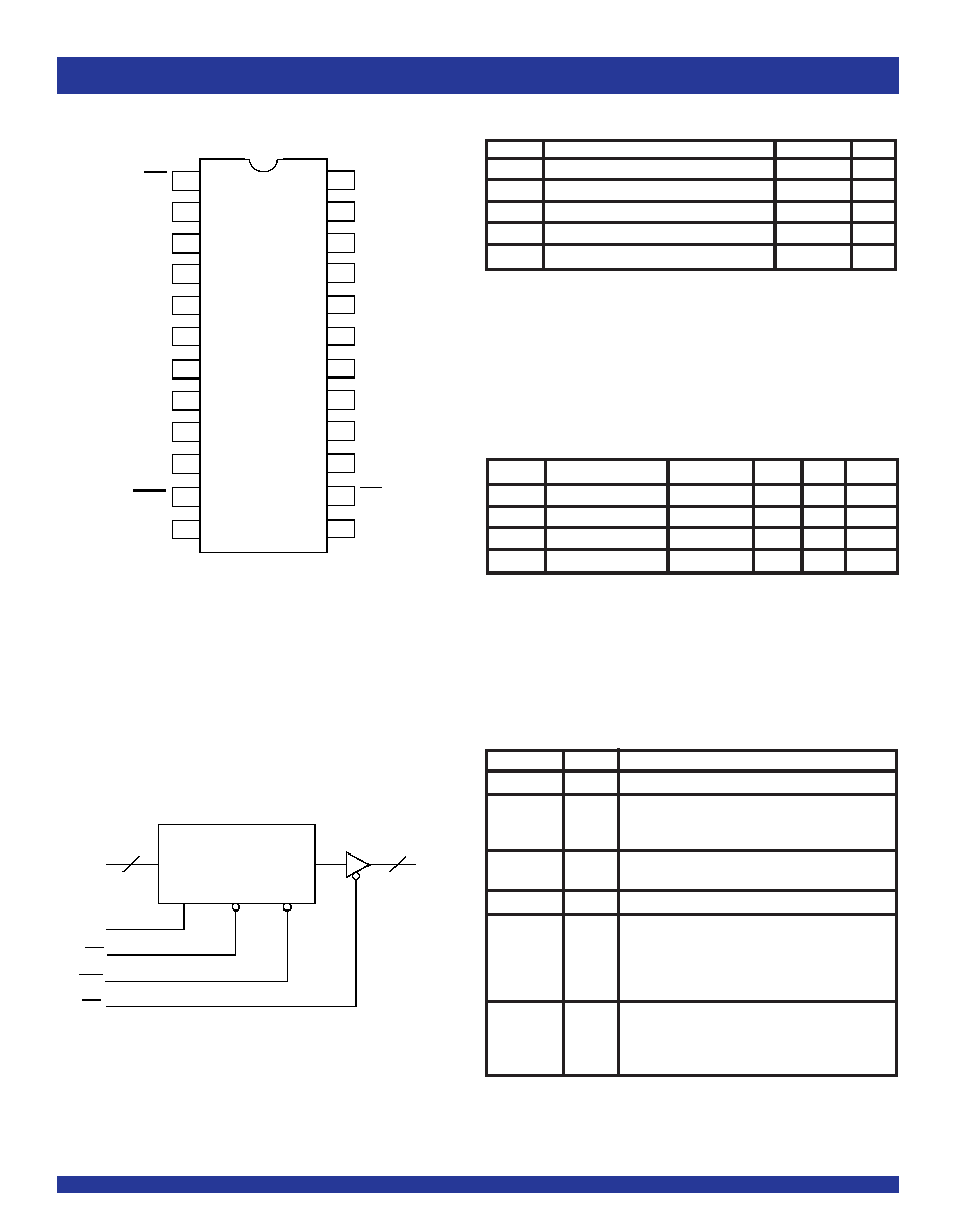
QSOP
TOP VIEW
PIN CONFIGURATION
Symbol
Description
Max
Unit
VTERM
Terminal Voltage with Respect to GND
–0.5 to +7
V
TSTG
Storage Temperature
–65 to +150
°C
IOUT
DC Output Current Max Sink Current/Pin
120
mA
IIK
Input Diode Current, VIN < 0
–20
mA
IOK
Output Diode Current, VOUT < 0
–50
mA
ABSOLUTE MAXIMUM RATINGS(1)
NOTE:
1. Stresses greater than those listed under ABSOLUTE MAXIMUM RATINGS may cause
permanent damage to the device. This is a stress rating only and functional operation
of the device at these or any other conditions above those indicated in the operational
sections of this specification is not implied. Exposure to absolute maximum rating
conditions for extended periods may affect reliability.
CAPACITANCE (TA = +25°C, F = 1.0MHz)
NOTES:
1. This parameter is measured at characterization but not tested.
2. Pins 1, 3-11, 13.
3. Pin 2.
4. Pins 15-22.
5. Pins 14, 23.
PIN DESCRIPTION
Pin Names
I/O
Description
Dx
I
DFlip-FlopDataInputs
CLR
I
When the clear input is LOW and OE is LOW, the Yx
outputsareLOW. WhenclearinputisHIGH,datacan
beenteredintotheregister.
C P
I
ClockPulsefortheregister. Entersdataintotheregister
ontheLOW-to-HIGHtransition.
Y x
O
Register3-StateOutputs
E N
I
Clock Enable. When the clock enable is LOW, data
on the Dx input is transferred to the Yx output on the
LOW-to-HIGH clock transition. When the clock
enable is HIGH, the Yx outputs do not change state,
regardlessofthedataorclockinputtransitions.
OE
I
Output Control. When the OE input is HIGH, the Yx
outputsareinthehighimpedancestate. WhentheOE
input is LOW, the TRUE register data is present at the
Yx outputs.
Symbol
Parameter(1)
Conditions
Typ.
Max.
Unit
CIN(2)
Input Capacitance
VIN = 0V
4
—
pF
CIN(3)
Input Capacitance
VIN = 0V
8
—
pF
COUT(4)
Output Capacitance
VOUT = 0V
6
—
pF
COUT(5)
Output Capacitance
VOUT = 0V
8
—
pF
LOGIC SYMBOL
D4
D5
D3
D7
D6
D1
D2
D8
GND
OE
D0
CLR
2
3
1
VCC
20
19
18
15
16
23
22
24
21
17
Y2
Y4
Y3
Y6
Y5
Y1
Y7
Y8
13
14
CP
EN
Y0
9
10
5
6
7
4
8
11
12
Dx
CP
EN
CLR
OE
DQ
Yx
CP
EN
CLR
9
相关PDF资料 |
PDF描述 |
|---|---|
| QS74FCT2823ATQ8 | FCT SERIES, 9-BIT DRIVER, TRUE OUTPUT, PDSO24 |
| QS74FCT2823BTQ | FCT SERIES, 9-BIT DRIVER, TRUE OUTPUT, PDSO24 |
| QS74FCT2823BTQ8 | FCT SERIES, 9-BIT DRIVER, TRUE OUTPUT, PDSO24 |
| QS5805ATQ | LOW SKEW CLOCK DRIVER, 5 TRUE OUTPUT(S), 0 INVERTED OUTPUT(S), PDSO20 |
| QS5805ATSO | LOW SKEW CLOCK DRIVER, 5 TRUE OUTPUT(S), 0 INVERTED OUTPUT(S), PDSO20 |
相关代理商/技术参数 |
参数描述 |
|---|---|
| QS74FCT2823ATQX | 制造商:未知厂家 制造商全称:未知厂家 功能描述:9-Bit D-Type Flip-Flop |
| QS74FCT2823ATSO | 制造商:未知厂家 制造商全称:未知厂家 功能描述:9-Bit D-Type Flip-Flop |
| QS74FCT2823ATSOX | 制造商:未知厂家 制造商全称:未知厂家 功能描述:9-Bit D-Type Flip-Flop |
| QS74FCT2823BTP | 制造商:Rochester Electronics LLC 功能描述:- Bulk 制造商:Integrated Device Technology Inc 功能描述: |
| QS74FCT2823BTQ | 制造商:未知厂家 制造商全称:未知厂家 功能描述:9-Bit D-Type Flip-Flop |
发布紧急采购,3分钟左右您将得到回复。