- 您现在的位置:买卖IC网 > PDF目录380636 > R1Q2A3609ABG-40R (Renesas Technology Corp.) 36-Mbit QDR™II SRAM 2-word Burst PDF资料下载
参数资料
| 型号: | R1Q2A3609ABG-40R |
| 厂商: | Renesas Technology Corp. |
| 英文描述: | 36-Mbit QDR™II SRAM 2-word Burst |
| 文件页数: | 11/25页 |
| 文件大小: | 394K |
| 代理商: | R1Q2A3609ABG-40R |
R1Q2A3636/R1Q2A3618/R1Q2A3609
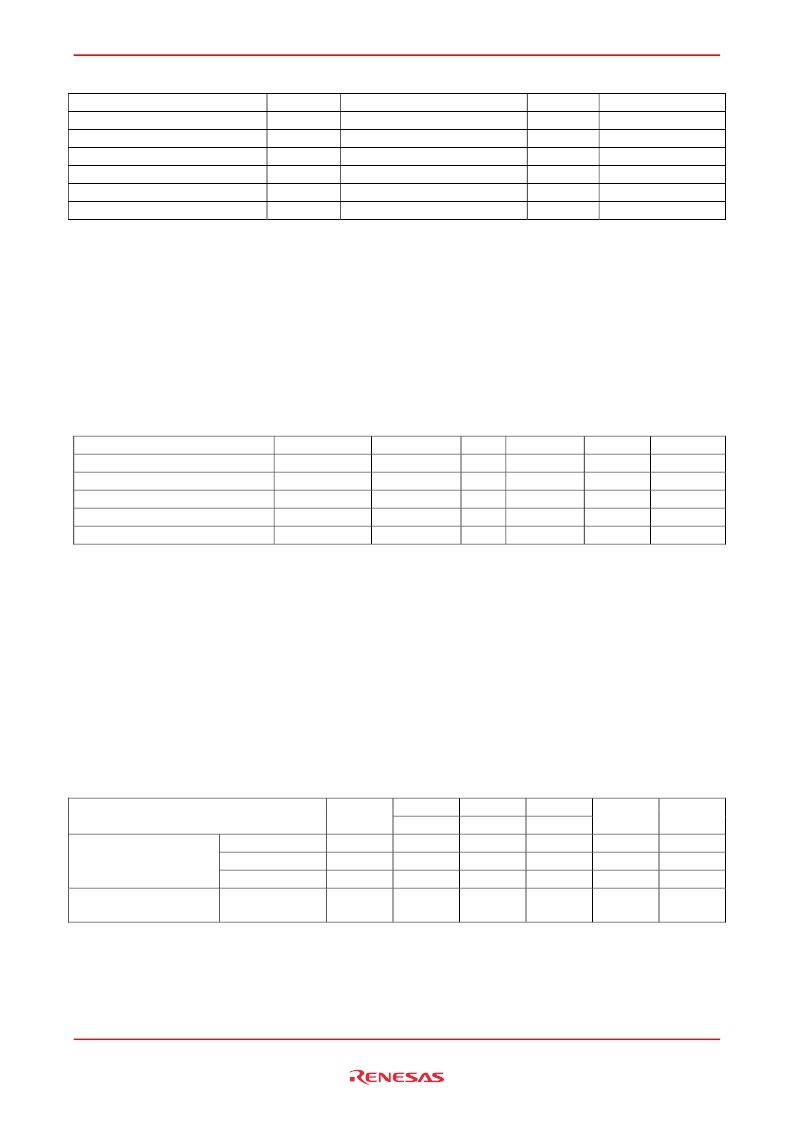
Absolute Maximum Ratings
Parameter
Symbol
V
IN
V
I/O
V
DD
V
DDQ
Tj
T
STG
Rating
Unit
V
V
V
V
°C
°C
Notes
Input voltage on any ball
Input/output voltage
Core supply voltage
Output supply voltage
Junction temperature
Storage temperature
Notes: 1. All voltage is referenced to V
SS
.
2. Permanent device damage may occur if Absolute Maximum Ratings are exceeded. Functional operation
should be restricted the Operation Conditions. Exposure to higher than recommended voltages for extended
periods of time could affect device reliability.
3. These CMOS memory circuits have been designed to meet the DC and AC specifications shown in the tables
after thermal equilibrium has been established.
4. The following supply voltage application sequence is recommended: V
SS
, V
DD
, V
DDQ
, V
REF
then V
IN
.
Remember, according to the Absolute Maximum Ratings table, V
DDQ
is not to exceed 2.5 V, whatever the
instantaneous value of V
DDQ
.
Recommended DC Operating Conditions
0.5 to V
DD
+ 0.5 (2.5 V max.)
0.5 to V
DDQ
+ 0.5 (2.5 V max.)
0.5 to 2.5
0.5 to V
DD
+125 (max)
55 to +125
1, 4
1, 4
1, 4
1, 4
(Ta = 0 to +70°C)
Unit
V
V
V
1
V
2, 3
V
2, 3
Parameter
Symbol
V
DD
V
DDQ
V
REF
V
IH (DC)
V
IL (DC)
Min
1.7
1.4
0.68
Typ
1.8
1.5
0.75
Max
1.9
V
DD
0.95
Notes
Power supply voltage --core
Power supply voltage --I/O
Input reference voltage --I/O
Input high voltage
Input low voltage
Notes: 1. Peak to peak AC component superimposed on V
REF
may not exceed 5% of V
REF
.
2. Overshoot: V
IH (AC)
≤
V
DDQ
+ 0.5 V for t
≤
t
KHKH
/2
Undershoot: V
IL (AC)
≥
0.5 V for t
≤
t
KHKH
/2
Power-up: V
IH
≤
V
DDQ
+ 0.3 V and V
DD
≤
1.7 V and V
DDQ
≤
1.4 V for t
≤
200 ms
During normal operation, V
DDQ
must not exceed V
DD
.
Control input signals may not have pulse widths less than t
KHKL
(min) or operate at cycle rates less than
t
KHKH
(min).
During normal operation, V
IH(DC)
must not exceed V
DDQ
and V
IL(DC)
must not be lower than V
SS
.
3. These are DC test criteria. The AC V
IH
/ V
IL
levels are defined separately to measure timing parameters.
V
REF
+
0.1
0.3
V
DDQ
+
0.3
V
REF
0.1
DC Characteristics
(Ta = 0 to +70
°
C, V
DD
= 1.8V
±
0.1V)
60
Max
Unit
500
550
600
330
40
Max
600
650
700
350
50
Max
550
600
650
340
Parameter
Symbol
I
DD
I
DD
I
DD
I
SB1
Notes
1, 2, 3
1, 2, 3
1, 2, 3
2, 4, 5
(×9)
(×18)
(×36)
mA
mA
mA
mA
Operating supply current
(READ / WRITE)
Standby supply current
(NOP)
(×9 / ×18 / ×36)
REJ03C0294-0003 Rev.0.03 Jul. 31, 2007
Page 11 of 23
相关PDF资料 |
PDF描述 |
|---|---|
| R1Q2A3609ABG-50R | 36-Mbit QDR™II SRAM 2-word Burst |
| R1Q2A3609ABG-60R | 36-Mbit QDR™II SRAM 2-word Burst |
| R1Q2A3618 | 36-Mbit QDR™II SRAM 2-word Burst |
| R1Q2A3618ABG-40R | 36-Mbit QDR™II SRAM 2-word Burst |
| R1Q2A3618ABG-50R | 36-Mbit QDR™II SRAM 2-word Burst |
相关代理商/技术参数 |
参数描述 |
|---|---|
| R1Q2A3609ABG40RB0 | 制造商:RENESAS 制造商全称:Renesas Technology Corp 功能描述:36-Mbit QDR?II SRAM 2-word Burst |
| R1Q2A3609ABG40RS0 | 制造商:RENESAS 制造商全称:Renesas Technology Corp 功能描述:36-Mbit QDR?II SRAM 2-word Burst |
| R1Q2A3609ABG40RT0 | 制造商:RENESAS 制造商全称:Renesas Technology Corp 功能描述:36-Mbit QDR?II SRAM 2-word Burst |
| R1Q2A3609ABG-50R | 制造商:RENESAS 制造商全称:Renesas Technology Corp 功能描述:36-Mbit QDR™II SRAM 2-word Burst |
| R1Q2A3609ABG50RB0 | 制造商:RENESAS 制造商全称:Renesas Technology Corp 功能描述:36-Mbit QDR?II SRAM 2-word Burst |
发布紧急采购,3分钟左右您将得到回复。