- 您现在的位置:买卖IC网 > PDF目录270824 > R3111H391A-T1 (RICOH COMPANY LTD) 1-CHANNEL POWER SUPPLY SUPPORT CKT, PSSO3 PDF资料下载
参数资料
| 型号: | R3111H391A-T1 |
| 厂商: | RICOH COMPANY LTD |
| 元件分类: | 电源管理 |
| 英文描述: | 1-CHANNEL POWER SUPPLY SUPPORT CKT, PSSO3 |
| 封装: | SOT-89, 3 PIN |
| 文件页数: | 22/22页 |
| 文件大小: | 195K |
| 代理商: | R3111H391A-T1 |
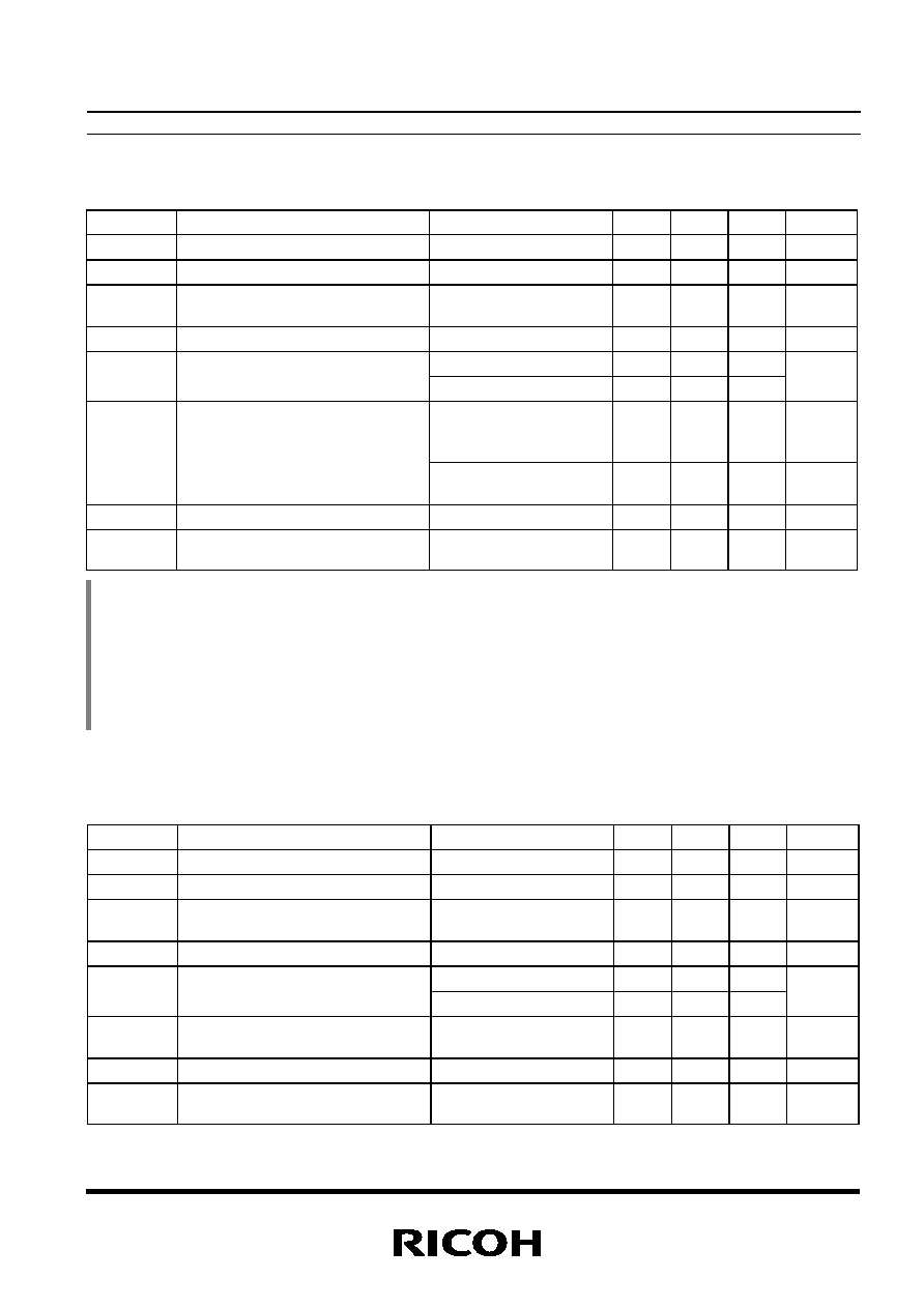
R3111x
9
R3111x54xA/C
Topt
=25°C
Symbol
Item
Conditions
Min.
Typ.
Max.
Unit
VDET
Detector Threshold
5.292
5.400
5.508
V
VHYS
Detector Threshold Hysteresis
0.162
0.270
0.378
V
ISS
Supply Current
VDD
= 5.20V
7.40V
1.2
1.4
3.6
4.2
A
VDDH
Maximum Operating Voltage
10
V
Topt
=25°C
0.55
0.70
VDDL
Minimum Operating Voltage
Note1
40°C <= Topt <= 85°C
0.65
0.80
V
Nch
VDS
=0.05V, VDD=0.70V
VDS
=0.50V, VDD=1.50V
0.01
1.00
0.05
2.00
mA
IOUT
Output Current
(Driver Output Pin)
Pch
VDS
=2.1V, VDD=8.0V
1.5
3.0
mA
tPLH
Output Delay Time
Note2
100
s
VDET/T
Detector Threshold Temperature
Coefficient
40°C <= Topt <= 85°C
±100
ppm/
°C
Note1: Minimum operating voltage means the value of input voltage when output voltage maintains 0.1V or less. (In
the case of Nch Open Drain Output type, the output pin is pulled up with a resistance of 470k
to 5.0V.)
Note2: In the case of CMOS Output type: The time interval between the rising edge of VDD input pulse from 0.7V
to (
+VDET)+2.0V and output voltage level becoming to VDD/2.
In the case of Nch Open Drain Output type: the output pin is pulled up with a resistance of 470k
to
5.0V, The time interval between the rising edge of VDD input pulse from 0.7V to (
+VDET)+2.0V and output
voltage level becoming to 2.5V.
R3111Q231B
Topt
=25°C
Symbol
Item
Conditions
Min.
Typ.
Max.
Unit
VDET
Detector Threshold
2.254
2.300
2.346
V
VHYS
Detector Threshold Hysteresis
0.069
0.115
0.161
V
ISS
Supply Current
VDD
=2.20V
4.30V
0.9
1.1
2.7
3.3
A
VDDH
Maximum Operating Voltage
10
V
Topt
=25°C
0.55
0.70
VDDL
Minimum Operating Voltage
Note1
40°C <= Topt <= 85°C
0.65
0.80
V
IOUT
Output Current (Driver Output Pin)
Nch
VDS
=0.50V,VDD=3.00V
10
mA
PLH
Output Delay Time
Note2
100
s
VDET/T
Detector Threshold Temperature
Coefficient
40°C <= Topt <= 85°C
±100
ppm/
°C
相关PDF资料 |
PDF描述 |
|---|---|
| R3111Q131C-TR | 1-CHANNEL POWER SUPPLY SUPPORT CKT, PDSO4 |
| R3111Q481A-TR | 1-CHANNEL POWER SUPPLY SUPPORT CKT, PDSO4 |
| RN5VT12CC-TR | POWER SUPPLY SUPPORT CKT, PDSO5 |
| RN5VT15CA | POWER SUPPLY SUPPORT CKT, PDSO5 |
| RN5VT22AC | POWER SUPPLY SUPPORT CKT, PDSO5 |
相关代理商/技术参数 |
参数描述 |
|---|---|
| R3111H391C | 制造商:RICOH 制造商全称:RICOH electronics devices division 功能描述:POWER MANAGEMENT ICs MARK INFORMATIONS R3111H SERIES MARK SPECIFICATION |
| R3111H4.01A- | 制造商:未知厂家 制造商全称:未知厂家 功能描述:Analog IC |
| R3111H4.01A-TR | 制造商:未知厂家 制造商全称:未知厂家 功能描述:Analog IC |
| R3111H4.01C- | 制造商:未知厂家 制造商全称:未知厂家 功能描述:Analog IC |
| R3111H4.01C-TR | 制造商:未知厂家 制造商全称:未知厂家 功能描述:Analog IC |
发布紧急采购,3分钟左右您将得到回复。