- 您现在的位置:买卖IC网 > PDF目录69309 > R5F21365ANFP 8-BIT, FLASH, 20 MHz, MICROCONTROLLER, PQFP64 PDF资料下载
参数资料
| 型号: | R5F21365ANFP |
| 元件分类: | 微控制器/微处理器 |
| 英文描述: | 8-BIT, FLASH, 20 MHz, MICROCONTROLLER, PQFP64 |
| 封装: | 10 X 10 MM, 0.50 MM PITCH, PLASTIC, LQFP-64 |
| 文件页数: | 28/57页 |
| 文件大小: | 477K |
| 代理商: | R5F21365ANFP |
第1页第2页第3页第4页第5页第6页第7页第8页第9页第10页第11页第12页第13页第14页第15页第16页第17页第18页第19页第20页第21页第22页第23页第24页第25页第26页第27页当前第28页第29页第30页第31页第32页第33页第34页第35页第36页第37页第38页第39页第40页第41页第42页第43页第44页第45页第46页第47页第48页第49页第50页第51页第52页第53页第54页第55页第56页第57页
R8C/36A Group
5. Electrical Characteristics
REJ03B0265-0110 Rev.1.10 Sep 28, 2009
Page 34 of 55
Under development Preliminary specification
Specifications in this manual are tentative and subject to change.
Notes:
1. The measurement condition is VCC = 1.8 to 5.5 V and Topr =
20 to 85°C (N version).
2. Select the voltage detection level with bits VDSEL0 and VDSEL1 in the OFS register.
3. Necessary time until the voltage detection circuit operates when setting to 1 again after setting the VCA25 bit in the VCA2
register to 0.
4. Time until the voltage monitor 0 reset is generated after the voltage passes Vdet0.
Notes:
1. The measurement condition is VCC = 1.8 to 5.5 V and Topr =
20 to 85°C (N version).
2. Select the voltage detection level with bits VD1S0 to VD1S3 in the VD1LS register.
3. Time until the voltage monitor 1 interrupt request is generated after the voltage passes Vdet1.
4. Necessary time until the voltage detection circuit operates when setting to 1 again after setting the VCA26 bit in the VCA2
register to 0.
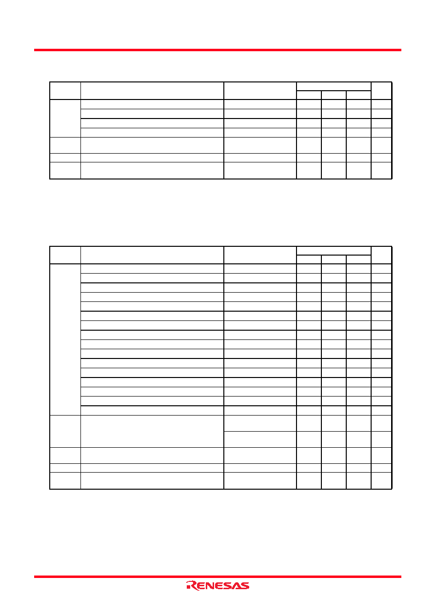
Table 5.9
Voltage Detection 0 Circuit Electrical Characteristics
Symbol
Parameter
Condition
Standard
Unit
Min.
Typ.
Max.
Vdet0
Voltage detection level Vdet0_0 (2)
1.80
1.90
2.05
V
Voltage detection level Vdet0_1 (2)
2.15
2.35
2.50
V
Voltage detection level Vdet0_2 (2)
2.65
2.85
3.00
V
Voltage detection level Vdet0_3 (2)
3.55
3.80
4.05
V
—
Voltage detection 0 circuit response time (4)
At the falling of VCC from
5.0 V to (Vdet0_0
0.1) V
—
6
150
s
—
Voltage detection circuit self power consumption
VCA25 = 1, VCC = 5.0 V
—
1.5
—
A
td(E-A)
Waiting time until voltage detection circuit operation
starts (3)
—
100
s
Table 5.10
Voltage Detection 1 Circuit Electrical Characteristics
Symbol
Parameter
Condition
Standard
Unit
Min.
Typ.
Max.
Vdet1
Voltage detection level Vdet1_0 (2)
At the falling of VCC
2.00
2.20
2.40
V
Voltage detection level Vdet1_1 (2)
At the falling of VCC
2.15
2.35
2.55
V
Voltage detection level Vdet1_2 (2)
At the falling of VCC
2.30
2.50
2.70
V
Voltage detection level Vdet1_3 (2)
At the falling of VCC
2.45
2.65
2.85
V
Voltage detection level Vdet1_4 (2)
At the falling of VCC
2.60
2.80
3.00
V
Voltage detection level Vdet1_5 (2)
At the falling of VCC
2.75
2.95
3.15
V
Voltage detection level Vdet1_6 (2)
At the falling of VCC
2.90
3.10
3.30
V
Voltage detection level Vdet1_7 (2)
At the falling of VCC
3.05
3.25
3.45
V
Voltage detection level Vdet1_8 (2)
At the falling of VCC
3.20
3.40
3.60
V
Voltage detection level Vdet1_9 (2)
At the falling of VCC
3.35
3.55
3.75
V
Voltage detection level Vdet1_A (2)
At the falling of VCC
3.50
3.70
3.90
V
Voltage detection level Vdet1_B (2)
At the falling of VCC
3.65
3.85
4.05
V
Voltage detection level Vdet1_C (2)
At the falling of VCC
3.80
4.00
4.20
V
Voltage detection level Vdet1_D (2)
At the falling of VCC
3.95
4.15
4.35
V
Voltage detection level Vdet1_E (2)
At the falling of VCC
4.10
4.30
4.50
V
Voltage detection level Vdet1_F (2)
At the falling of VCC
4.25
4.45
4.65
V
—
Hysteresis width at the rising of VCC in voltage
detection 1 circuit
Vdet1_0 to Vdet1_5
selected
—0.07—
V
Vdet1_6 to Vdet1_F
selected
—0.10—
V
—
Voltage detection 1 circuit response time (3)
At the falling of VCC from
5.0 V to (Vdet1_0
0.1) V
—
60
150
s
—
Voltage detection circuit self power consumption
VCA26 = 1, VCC = 5.0 V
—
1.7
—
A
td(E-A)
Waiting time until voltage detection circuit operation
starts (4)
—
100
s
相关PDF资料 |
PDF描述 |
|---|---|
| R5F21368FKFP | 32-BIT, FLASH, 20 MHz, MICROCONTROLLER, PQFP64 |
| R5F2136CEJFP | 32-BIT, FLASH, 20 MHz, MICROCONTROLLER, PQFP64 |
| R5F2136AEJFP | 32-BIT, FLASH, 20 MHz, MICROCONTROLLER, PQFP64 |
| R5F2136CFKFP | 32-BIT, FLASH, 20 MHz, MICROCONTROLLER, PQFP64 |
| R5F2136CGJFP | 32-BIT, FLASH, 20 MHz, MICROCONTROLLER, PQFP64 |
相关代理商/技术参数 |
参数描述 |
|---|---|
| R5F21365CDFA | 制造商:RENESAS 制造商全称:Renesas Technology Corp 功能描述:RENESAS MCU |
| R5F21365CDFA#30 | 制造商:Renesas Electronics Corporation 功能描述:IC MCU 16BIT 24KB FLASH 64LQFP |
| R5F21365CDFA#V0 | 功能描述:MCU 24KB ROM 2KB RAM 64-LQFP RoHS:是 类别:集成电路 (IC) >> 嵌入式 - 微控制器, 系列:R8C/3x/36C 标准包装:250 系列:80C 核心处理器:8051 芯体尺寸:8-位 速度:16MHz 连通性:EBI/EMI,I²C,UART/USART 外围设备:POR,PWM,WDT 输入/输出数:40 程序存储器容量:- 程序存储器类型:ROMless EEPROM 大小:- RAM 容量:256 x 8 电压 - 电源 (Vcc/Vdd):4.5 V ~ 5.5 V 数据转换器:A/D 8x10b 振荡器型:内部 工作温度:-40°C ~ 85°C 封装/外壳:68-LCC(J 形引线) 包装:带卷 (TR) |
| R5F21365CDFP | 制造商:RENESAS 制造商全称:Renesas Technology Corp 功能描述:RENESAS MCU |
| R5F21365CNFA | 制造商:RENESAS 制造商全称:Renesas Technology Corp 功能描述:RENESAS MCU |
发布紧急采购,3分钟左右您将得到回复。