- 您现在的位置:买卖IC网 > PDF目录69310 > R5F21388HKFP FLASH, 20 MHz, MICROCONTROLLER, PQFP80 PDF资料下载
参数资料
| 型号: | R5F21388HKFP |
| 元件分类: | 微控制器/微处理器 |
| 英文描述: | FLASH, 20 MHz, MICROCONTROLLER, PQFP80 |
| 封装: | 12 X 12 MM, 0.50 MM PITCH, PLASTIC, LQFP-80 |
| 文件页数: | 29/30页 |
| 文件大小: | 483K |
| 代理商: | R5F21388HKFP |
第1页第2页第3页第4页第5页第6页第7页第8页第9页第10页第11页第12页第13页第14页第15页第16页第17页第18页第19页第20页第21页第22页第23页第24页第25页第26页第27页第28页当前第29页第30页
87
ATmega165A/PA/325A/PA/3250A/PA/645A/P/6450A/P [DATASHEET]
8285E–AVR–02/2013
15.5.1
Force Output compare
In non-PWM waveform generation modes, the match output of the comparator can be forced by writing a one to
the Force Output Compare (FOC0A) bit. Forcing compare match will not set the OCF0A Flag or reload/clear the
timer, but the OC0A pin will be updated as if a real compare match had occurred (the COM0A1:0 bits settings
define whether the OC0A pin is set, cleared or toggled).
15.5.2
Compare Match Blocking by TCNT0 Write
All CPU write operations to the TCNT0 Register will block any compare match that occur in the next timer clock
cycle, even when the timer is stopped. This feature allows OCR0A to be initialized to the same value as TCNT0
without triggering an interrupt when the Timer/Counter clock is enabled.
15.5.3
Using the Output Compare Unit
Since writing TCNT0 in any mode of operation will block all compare matches for one timer clock cycle, there are
risks involved when changing TCNT0 when using the Output Compare unit, independently of whether the
Timer/Counter is running or not. If the value written to TCNT0 equals the OCR0A value, the compare match will be
missed, resulting in incorrect waveform generation. Similarly, do not write the TCNT0 value equal to BOTTOM
when the counter is down counting.
The setup of the OC0A should be performed before setting the Data Direction Register for the port pin to output.
The easiest way of setting the OC0A value is to use the Force Output Compare (FOC0A) strobe bits in Normal
mode. The OC0A Register keeps its value even when changing between Waveform Generation modes.
Be aware that the COM0A1:0 bits are not double buffered together with the compare value. Changing the
COM0A1:0 bits will take effect immediately.
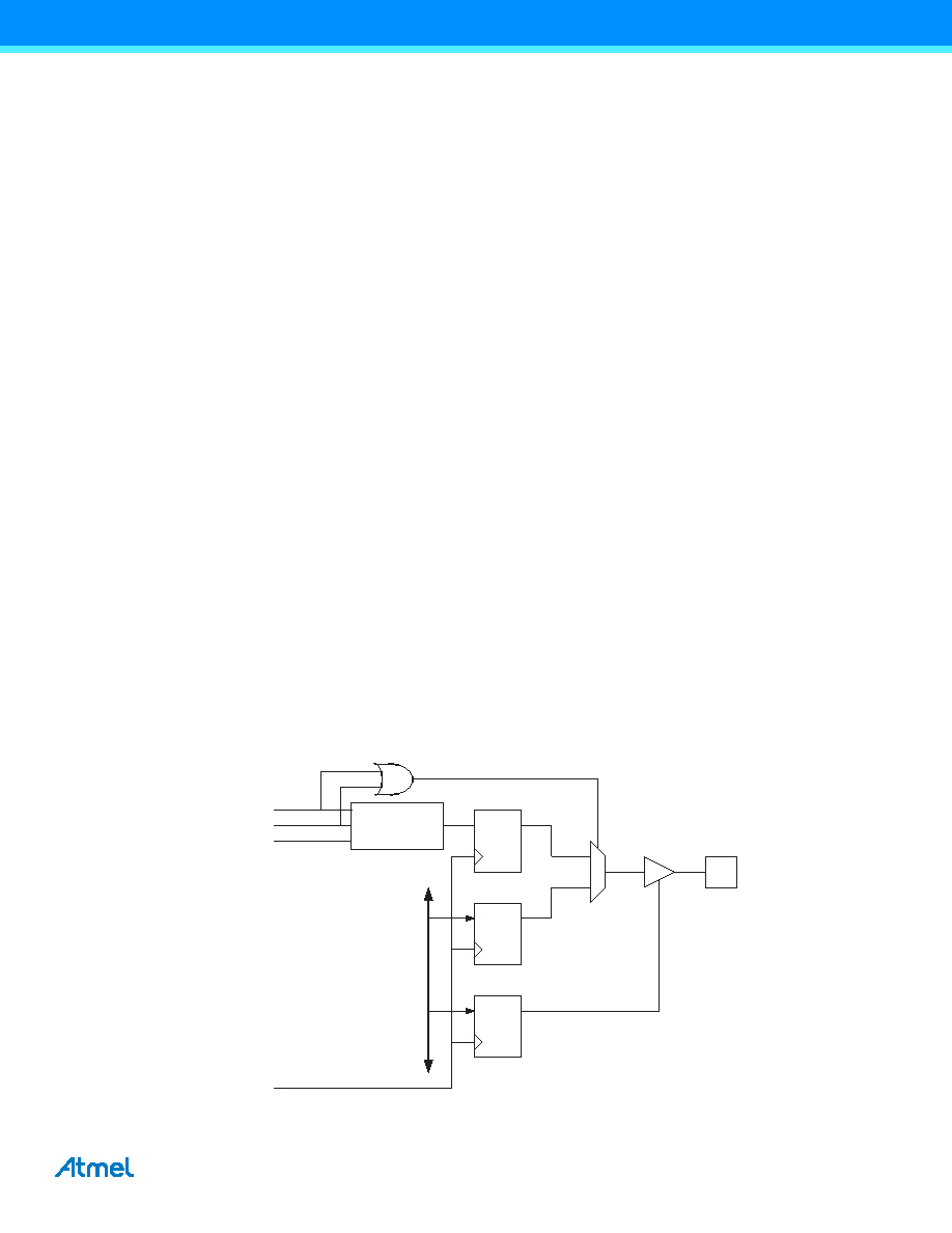
15.6
Compare Match Output Unit
The Compare Output mode (COM0A1:0) bits have two functions. The Waveform Generator uses the COM0A1:0
bits for defining the Output Compare (OC0A) state at the next compare match. Also, the COM0A1:0 bits control the
OC0A pin output source. Figure 15-4 shows a simplified schematic of the logic affected by the COM0A1:0 bit set-
ting. The I/O Registers, I/O bits, and I/O pins in the figure are shown in bold. Only the parts of the general I/O port
control registers (DDR and PORT) that are affected by the COM0A1:0 bits are shown. When referring to the OC0A
state, the reference is for the internal OC0A Register, not the OC0A pin. If a System Reset occur, the OC0A Reg-
ister is reset to “0”.
Figure 15-4. Compare Match Output Unit, schematic.
PORT
DDR
DQ
OCn
Pin
OCnx
DQ
Waveform
Generator
COMnx1
COMnx0
0
1
D
ATA
B
U
S
FOCn
clk
I/O
相关PDF资料 |
PDF描述 |
|---|---|
| R5F2138AFKFP | FLASH, 20 MHz, MICROCONTROLLER, PQFP80 |
| R5F2138AHJFP | FLASH, 20 MHz, MICROCONTROLLER, PQFP80 |
| R5F2138CFJFP | FLASH, 20 MHz, MICROCONTROLLER, PQFP80 |
| R5F2138CHJFP | FLASH, 20 MHz, MICROCONTROLLER, PQFP80 |
| R5F2138AFJFP | FLASH, 20 MHz, MICROCONTROLLER, PQFP80 |
相关代理商/技术参数 |
参数描述 |
|---|---|
| R5F21388MDFD | 制造商:RENESAS 制造商全称:Renesas Technology Corp 功能描述:The R8C/38M Group has data flash (1 KB × 4 blocks) with the background operation |
| R5F21388MDFP | 制造商:RENESAS 制造商全称:Renesas Technology Corp 功能描述:The R8C/38M Group has data flash (1 KB × 4 blocks) with the background operation |
| R5F21388MDFP#30 | 制造商:Renesas Electronics Corporation 功能描述:IC MCU 16BIT 64KB FLASH 80LQFP |
| R5F21388MDFP#V0 | 制造商:Renesas Electronics Corporation 功能描述:IC MCU 16BIT 64KB FLASH 80LQFP |
| R5F21388MDXXXFD | 制造商:RENESAS 制造商全称:Renesas Technology Corp 功能描述:The R8C/38M Group has data flash (1 KB × 4 blocks) with the background operation |
发布紧急采购,3分钟左右您将得到回复。