- 您现在的位置:买卖IC网 > PDF目录69310 > R5F2138AHJFP FLASH, 20 MHz, MICROCONTROLLER, PQFP80 PDF资料下载
参数资料
| 型号: | R5F2138AHJFP |
| 元件分类: | 微控制器/微处理器 |
| 英文描述: | FLASH, 20 MHz, MICROCONTROLLER, PQFP80 |
| 封装: | 12 X 12 MM, 0.50 MM PITCH, PLASTIC, LQFP-80 |
| 文件页数: | 4/30页 |
| 文件大小: | 483K |
| 代理商: | R5F2138AHJFP |
第1页第2页第3页当前第4页第5页第6页第7页第8页第9页第10页第11页第12页第13页第14页第15页第16页第17页第18页第19页第20页第21页第22页第23页第24页第25页第26页第27页第28页第29页第30页
62
ATmega165A/PA/325A/PA/3250A/PA/645A/P/6450A/P [DATASHEET]
8285E–AVR–02/2013
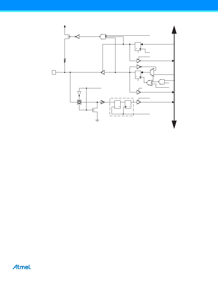
Figure 14-2. General digital I/O
Note:
1. WRx, WPx, WDx, RRx, RPx, and RDx are common to all pins within the same port. clkI/O, SLEEP, and PUD are
common to all ports.
14.2.1
Configuring the pin
Each port pin consists of three register bits: DDxn, PORTxn, and PINxn. As shown in ”Register description” on
page 80, the DDxn bits are accessed at the DDRx I/O address, the PORTxn bits at the PORTx I/O address, and
the PINxn bits at the PINx I/O address.
The DDxn bit in the DDRx Register selects the direction of this pin. If DDxn is written logic one, Pxn is configured
as an output pin. If DDxn is written logic zero, Pxn is configured as an input pin.
If PORTxn is written logic one when the pin is configured as an input pin, the pull-up resistor is activated. To switch
the pull-up resistor off, PORTxn has to be written logic zero or the pin has to be configured as an output pin. The
port pins are tri-stated when reset condition becomes active, even if no clocks are running.
If PORTxn is written logic one when the pin is configured as an output pin, the port pin is driven high (one). If
PORTxn is written logic zero when the pin is configured as an output pin, the port pin is driven low (zero).
14.2.2
Toggling the pin
Writing a logic one to PINxn toggles the value of PORTxn, independent on the value of DDRxn. Note that the SBI
instruction can be used to toggle one single bit in a port.
14.2.3
Switching between input and output
When switching between tri-state ({DDxn, PORTxn} = 0b00) and output high ({DDxn, PORTxn} = 0b11), an inter-
mediate state with either pull-up enabled {DDxn, PORTxn} = 0b01) or output low ({DDxn, PORTxn} = 0b10) must
occur. Normally, the pull-up enabled state is fully acceptable, as a high-impedant environment will not notice the
difference between a strong high driver and a pull-up. If this is not the case, the PUD bit in the MCUCR Register
can be set to disable all pull-ups in all ports.
clk
RPx
RRx
RDx
WDx
PUD
SYNCHRONIZER
WDx:
WRITE DDRx
WRx:
WRITE PORTx
RRx:
READ PORTx REGISTER
RPx:
READ PORTx PIN
PUD:
PULLUP DISABLE
clk
I/O:
I/O CLOCK
RDx:
READ DDRx
D
L
Q
RESET
Q
D
Q
D
CLR
PORTxn
Q
D
CLR
DDxn
PINxn
D
ATA
B
U
S
SLEEP
SLEEP:
SLEEP CONTROL
Pxn
I/O
WPx
0
1
WRx
WPx:
WRITE PINx REGISTER
相关PDF资料 |
PDF描述 |
|---|---|
| R5F2138CFJFP | FLASH, 20 MHz, MICROCONTROLLER, PQFP80 |
| R5F2138CHJFP | FLASH, 20 MHz, MICROCONTROLLER, PQFP80 |
| R5F2138AFJFP | FLASH, 20 MHz, MICROCONTROLLER, PQFP80 |
| R5F2138CCNFP | 8-BIT, FLASH, 20 MHz, MICROCONTROLLER, PQFP80 |
| R5F21386CNFP | 8-BIT, FLASH, 20 MHz, MICROCONTROLLER, PQFP80 |
相关代理商/技术参数 |
参数描述 |
|---|---|
| R5F2138AMDFD | 制造商:RENESAS 制造商全称:Renesas Technology Corp 功能描述:The R8C/38M Group has data flash (1 KB × 4 blocks) with the background operation |
| R5F2138AMDFP | 制造商:RENESAS 制造商全称:Renesas Technology Corp 功能描述:The R8C/38M Group has data flash (1 KB × 4 blocks) with the background operation |
| R5F2138AMDFP#V0 | 制造商:Renesas Electronics Corporation 功能描述:IC MCU 16BIT 96KB FLASH 80LQFP |
| R5F2138AMDXXXFD | 制造商:RENESAS 制造商全称:Renesas Technology Corp 功能描述:The R8C/38M Group has data flash (1 KB × 4 blocks) with the background operation |
| R5F2138AMDXXXFP | 制造商:RENESAS 制造商全称:Renesas Technology Corp 功能描述:The R8C/38M Group has data flash (1 KB × 4 blocks) with the background operation |
发布紧急采购,3分钟左右您将得到回复。