- 您现在的位置:买卖IC网 > PDF目录69310 > R5F213G2CNNP MICROCONTROLLER, QCC24 PDF资料下载
参数资料
| 型号: | R5F213G2CNNP |
| 元件分类: | 微控制器/微处理器 |
| 英文描述: | MICROCONTROLLER, QCC24 |
| 封装: | 4 X 4 MM, 0.50 MM PITCH, QFN-24 |
| 文件页数: | 2/59页 |
| 文件大小: | 654K |
| 代理商: | R5F213G2CNNP |
第1页当前第2页第3页第4页第5页第6页第7页第8页第9页第10页第11页第12页第13页第14页第15页第16页第17页第18页第19页第20页第21页第22页第23页第24页第25页第26页第27页第28页第29页第30页第31页第32页第33页第34页第35页第36页第37页第38页第39页第40页第41页第42页第43页第44页第45页第46页第47页第48页第49页第50页第51页第52页第53页第54页第55页第56页第57页第58页第59页
R8C/3GC Group
1. Overview
Under development Preliminary document
Specifications in this document are tentative and subject to change.
REJ03B0301-0010 Rev.0.10
Page 10 of 56
May 24, 2010
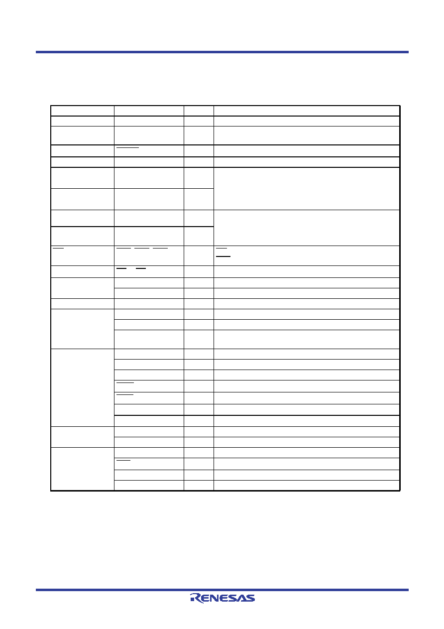
1.5
Pin Functions
I: Input
O: Output
I/O: Input and output
Note:
1. Refer to the oscillator manufacturer for oscillation characteristics.
Table 1.6
Pin Functions (1)
Item
Pin Name
I/O Type
Description
Power supply input VCC, VSS
Apply 1.8 V to 5.5 V to the VCC pin. Apply 0 V to the VSS pin.
Analog power
supply input
AVCC, AVSS
Power supply for the A/D converter.
Connect a capacitor between AVCC and AVSS.
Reset input
RESET
I
Input “L” on this pin resets the MCU.
MODE
I
Connect this pin to VCC via a resistor.
XIN clock input
XIN
I
These pins are provided for XIN clock generation circuit I/O.
Connect a ceramic resonator or a crystal oscillator between
the XIN and XOUT pins (1). To use an external clock, input it
to the XOUT pin and leave the XIN pin open.
XIN clock output
XOUT
I/O
XCIN clock input
XCIN
I
These pins are provided for XCIN clock generation circuit I/O.
Connect a crystal oscillator between the XCIN and XCOUT
pins (1). To use an external clock, input it to the XCIN pin and
leave the XCOUT pin open.
XCIN clock output
XCOUT
O
INT interrupt input
INT0, INT1, INT3
IINT interrupt input pins.
INT0 is timer RB, and RC input pin.
Key input interrupt
KI0 to KI3
I
Key input interrupt input pins
Timer RA
TRAIO
I/O
Timer RA I/O pin
TRAO
O
Timer RA output pin
Timer RB
TRBO
O
Timer RB output pin
Timer RC
TRCCLK
I
External clock input pin
TRCTRG
I
External trigger input pin
TRCIOA, TRCIOB,
TRCIOC, TRCIOD
I/O
Timer RC I/O pins
Serial interface
CLK0, CLK2
I/O
Transfer clock I/O pins
RXD0, RXD2
I
Serial data input pins
TXD0, TXD2
O
Serial data output pins
CTS2
I
Transmission control input pin
RTS2
O
Reception control output pin
SCL2
I/O
I2C mode clock I/O pin
SDA2
I/O
I2C mode data I/O pin
I2C bus
SCL
I/O
Clock I/O pin
SDA
I/O
Data I/O pin
SSU
SSI
I/O
Data I/O pin
SCS
I/O
Chip-select signal I/O pin
SSCK
I/O
Clock I/O pin
SSO
I/O
Data I/O pin
相关PDF资料 |
PDF描述 |
|---|---|
| R5F213G2MNNP | 8-BIT, FLASH, 20 MHz, MICROCONTROLLER, PQCC24 |
| R5F213G4DDSP | 8-BIT, FLASH, 20 MHz, MICROCONTROLLER, PDSO24 |
| R5F213G2DNSP | 8-BIT, FLASH, 20 MHz, MICROCONTROLLER, PDSO24 |
| R5F213G5DDSP | 8-BIT, FLASH, 20 MHz, MICROCONTROLLER, PDSO24 |
| R5F213J2CNNP | MICROCONTROLLER, QCC36 |
相关代理商/技术参数 |
参数描述 |
|---|---|
| R5F213G2CNNP#U0 | 制造商:Renesas Electronics Corporation 功能描述: 制造商:Renesas Electronics Corporation 功能描述:R8C3GC 8+2KB 1.8/5.5V -20 85C 24WQFN - Rail/Tube 制造商:Renesas Electronics Corporation 功能描述:16BIT MCU FLASH 8K 制造商:Renesas Electronics Corporation 功能描述:IC MCU 16BIT 8KB FLASH 24QFN |
| R5F213G2CNNP#V0 | 功能描述:MCU 8KB ROM 1KB RAM 24-WQFN RoHS:是 类别:集成电路 (IC) >> 嵌入式 - 微控制器, 系列:R8C/3x/3GC 标准包装:300 系列:78K0R/Ix3 核心处理器:78K/0R 芯体尺寸:16-位 速度:40MHz 连通性:3 线 SIO,I²C,LIN,UART/USART 外围设备:DMA,LVD,POR,PWM,WDT 输入/输出数:27 程序存储器容量:16KB(16K x 8) 程序存储器类型:闪存 EEPROM 大小:- RAM 容量:1K x 8 电压 - 电源 (Vcc/Vdd):2.7 V ~ 5.5 V 数据转换器:A/D 8x10b 振荡器型:内部 工作温度:-40°C ~ 85°C 封装/外壳:38-SSOP 包装:托盘 |
| R5F213G2CNSP | 制造商:RENESAS 制造商全称:Renesas Technology Corp 功能描述:RENESAS MCU |
| R5F213G2CNSP#U0 | 制造商:Renesas Electronics Corporation 功能描述:R8C3GC 8+2KB 1.8/5.5V -20 85C 24SSOP - Rail/Tube 制造商:Renesas Electronics Corporation 功能描述:IC MCU 16BIT 8KB FLASH 24SSOP |
| R5F213G2CNSP#W4 | 制造商:Renesas Electronics Corporation 功能描述:R8C3GC 8+2KB 1.8/5.5V -20 85C 24SSOP T&R - Tape and Reel 制造商:Renesas Electronics Corporation 功能描述:IC MCU 16BIT 8KB FLASH 24SSOP |
发布紧急采购,3分钟左右您将得到回复。