- 您现在的位置:买卖IC网 > PDF目录69310 > R5F213G6ADNP 8-BIT, FLASH, 20 MHz, MICROCONTROLLER, PQCC24 PDF资料下载
参数资料
| 型号: | R5F213G6ADNP |
| 元件分类: | 微控制器/微处理器 |
| 英文描述: | 8-BIT, FLASH, 20 MHz, MICROCONTROLLER, PQCC24 |
| 封装: | 4 X 4 MM, 0.50 MM PITCH, PLASTIC, QFN-24 |
| 文件页数: | 5/56页 |
| 文件大小: | 431K |
| 代理商: | R5F213G6ADNP |
第1页第2页第3页第4页当前第5页第6页第7页第8页第9页第10页第11页第12页第13页第14页第15页第16页第17页第18页第19页第20页第21页第22页第23页第24页第25页第26页第27页第28页第29页第30页第31页第32页第33页第34页第35页第36页第37页第38页第39页第40页第41页第42页第43页第44页第45页第46页第47页第48页第49页第50页第51页第52页第53页第54页第55页第56页
R8C/3GA Group
3. Memory
REJ03B0235-0110 Rev.1.10 Sep. 10, 2009
Page 13 of 53
3.
Memory
3.1
R8C/3GA Group
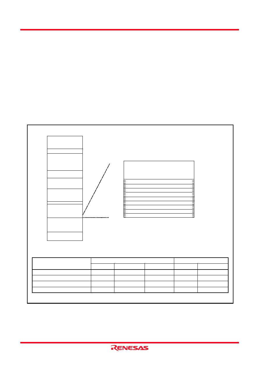
Figure 3.1 is a Memory Map of R8C/3GA Group. The R8C/3GA Group has a 1-Mbyte address space from
addresses 00000h to FFFFFh. The internal ROM (program ROM) is allocated lower addresses, beginning with
address 0FFFFh. For example, a 32-Kbyte internal ROM area is allocated addresses 08000h to 0FFFFh.
The fixed interrupt vector table is allocated addresses 0FFDCh to 0FFFFh. The starting address of each interrupt
routine is stored here.
The internal ROM (data flash) is allocated addresses 03000h to 03FFFh.
The internal RAM is allocated higher addresses, beginning with address 00400h. For example, a 2.5-Kbyte internal
RAM area is allocated addresses 00400h to 00DFFh. The internal RAM is used not only for data storage but also as
a stack area when a subroutine is called or when an interrupt request is acknowledged.
Special function registers (SFRs) are allocated addresses 00000h to 002FFh and 02C00h to 02FFFh. Peripheral
function control registers are allocated here. All unallocated spaces within the SFRs are reserved and cannot be
accessed by users.
Figure 3.1
Memory Map of R8C/3GA Group
0FFFFh
0FFDCh
Notes:
1. Data flash indicates block A (1 Kbyte), block B (1 Kbyte), block C (1 Kbyte) and block D (1 Kbyte).
2. The blank areas are reserved and cannot be accessed by users.
FFFFFh
0FFFFh
0YYYYh
0XXXXh
00400h
002FFh
00000h
Internal ROM
(program ROM)
Internal RAM
SFR
(Refer to 4. Special
Function Registers
(SFRs))
02FFFh
02C00h
SFR
(Refer to 4. Special Function
Registers (SFRs))
ZZZZZh
Internal ROM
(program ROM)
03FFFh
03000h
Internal ROM
(data flash) (1)
0FFD8h
Reserved area
Undefined instruction
Overflow
BRK instruction
Address match
Single step
Watchdog timer, oscillation stop detection, voltage monitor
Address break
(Reserved)
Reset
Part Number
R5F213G2ANNP, R5F213G2ADNP
R5F213G4ANNP, R5F213G4ADNP
R5F213G5ANNP, R5F213G5ADNP
R5F213G6ANNP, R5F213G6ADNP
Internal ROM
Internal RAM
Size
Address 0YYYYh
Size
Address 0XXXXh
Address ZZZZZh
8 Kbytes
16 Kbytes
24 Kbytes
32 Kbytes
0E000h
0C000h
0A000h
08000h
1 Kbyte
1.5 Kbytes
2 Kbytes
2.5 Kbytes
007FFh
009FFh
00BFFh
00DFFh
–
相关PDF资料 |
PDF描述 |
|---|---|
| R5F213G2CNNP | MICROCONTROLLER, QCC24 |
| R5F213G2MNNP | 8-BIT, FLASH, 20 MHz, MICROCONTROLLER, PQCC24 |
| R5F213G4DDSP | 8-BIT, FLASH, 20 MHz, MICROCONTROLLER, PDSO24 |
| R5F213G2DNSP | 8-BIT, FLASH, 20 MHz, MICROCONTROLLER, PDSO24 |
| R5F213G5DDSP | 8-BIT, FLASH, 20 MHz, MICROCONTROLLER, PDSO24 |
相关代理商/技术参数 |
参数描述 |
|---|---|
| R5F213G6ANNP | 制造商:RENESAS 制造商全称:Renesas Technology Corp 功能描述:RENESAS MCU |
| R5F213G6CDNP | 制造商:RENESAS 制造商全称:Renesas Technology Corp 功能描述:RENESAS MCU |
| R5F213G6CDSP | 制造商:RENESAS 制造商全称:Renesas Technology Corp 功能描述:RENESAS MCU |
| R5F213G6CDSP#U0 | 制造商:Renesas Electronics Corporation 功能描述:R8C3GC 32+4KB 1.8/5.5V -40 85C 24SSOP - Rail/Tube 制造商:Renesas Electronics Corporation 功能描述:IC MCU 16BIT 32KB FLASH 24SSOP |
| R5F213G6CDSP#V0 | 功能描述:MCU 32KB ROM 2.5KB RAM 24-SSOP RoHS:是 类别:集成电路 (IC) >> 嵌入式 - 微控制器, 系列:R8C/3x/3GC 标准包装:250 系列:80C 核心处理器:8051 芯体尺寸:8-位 速度:16MHz 连通性:EBI/EMI,I²C,UART/USART 外围设备:POR,PWM,WDT 输入/输出数:40 程序存储器容量:- 程序存储器类型:ROMless EEPROM 大小:- RAM 容量:256 x 8 电压 - 电源 (Vcc/Vdd):4.5 V ~ 5.5 V 数据转换器:A/D 8x10b 振荡器型:内部 工作温度:-40°C ~ 85°C 封装/外壳:68-LCC(J 形引线) 包装:带卷 (TR) |
发布紧急采购,3分钟左右您将得到回复。