- 您现在的位置:买卖IC网 > PDF目录69311 > R5F2L38ABDFP 8-BIT, FLASH, 20 MHz, MICROCONTROLLER, PQFP80 PDF资料下载
参数资料
| 型号: | R5F2L38ABDFP |
| 元件分类: | 微控制器/微处理器 |
| 英文描述: | 8-BIT, FLASH, 20 MHz, MICROCONTROLLER, PQFP80 |
| 封装: | 12 X 12 MM, 0.50 MM PITCH, PLASTIC, LQFP-80 |
| 文件页数: | 48/89页 |
| 文件大小: | 1350K |
| 代理商: | R5F2L38ABDFP |
第1页第2页第3页第4页第5页第6页第7页第8页第9页第10页第11页第12页第13页第14页第15页第16页第17页第18页第19页第20页第21页第22页第23页第24页第25页第26页第27页第28页第29页第30页第31页第32页第33页第34页第35页第36页第37页第38页第39页第40页第41页第42页第43页第44页第45页第46页第47页当前第48页第49页第50页第51页第52页第53页第54页第55页第56页第57页第58页第59页第60页第61页第62页第63页第64页第65页第66页第67页第68页第69页第70页第71页第72页第73页第74页第75页第76页第77页第78页第79页第80页第81页第82页第83页第84页第85页第86页第87页第88页第89页
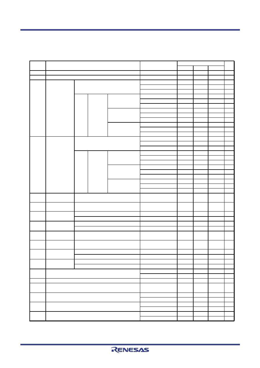
5. Electrical Characteristics
REJ03B0243-0030 Rev.0.30
Jan 21, 2009
Page 50 of 76
R8C/L35A Group, R8C/L36A Group, R8C/L38A Group, R8C/L3AA Group,
R8C/L35B Group, R8C/L36B Group, R8C/L38B Group, R8C/L3AB Group
Under development Preliminary specification
Specifications in this manual are tentative and subject to change.
5.2
Recommended Operating Conditions
Notes:
1.
The average output current indicates the average value of current measured during 100 ms.
2.
This applies when the drive capacity of the output transistor is set to High by registers P10DRR and P11DRR. When the drive
capacity is set to Low, the value of any other pin applies.
3.
fOCO40M can be used as the count source for timer RC, timer RD, or timer RG in the range of VCC = 2.7 V to 5.5V.
Table 5.2
Recommended Operating Conditions
(VCC = 1.8 to 5.5 V and Topr =
20 to 85°C (N version) / 40 to 85°C (D version), unless
otherwise specified.)
Symbol
Parameter
Conditions
Standard
Unit
Min.
Typ.
Max.
VCC/AVCC Supply voltage
1.8
5.5
V
VSS/AVSS Supply voltage
0
V
VIH
Input “H” voltage Other than CMOS input
4.0 V
≤ VCC ≤ 5.5 V
0.8 VCC
VCC
V
2.7 V
≤ VCC < 4.0 V
0.8 VCC
VCC
V
1.8 V
≤ VCC < 2.7 V
0.9 VCC
VCC
V
CMOS
input
Input level
switching
function
(I/O port)
Input level selection
: 0.35 VCC
4.0 V
≤ VCC ≤ 5.5 V
0.5 VCC
VCC
V
2.7 V
≤ VCC < 4.0 V
0.55 VCC
VCC
V
1.8 V
≤ VCC < 2.7 V
0.65 VCC
VCC
V
Input level selection
: 0.5 VCC
4.0 V
≤ VCC ≤ 5.5 V
0.65 VCC
VCC
V
2.7 V
≤ VCC < 4.0 V
0.7 VCC
VCC
V
1.8 V
≤ VCC < 2.7 V
0.8 VCC
VCC
V
Input level selection
: 0.7 VCC
4.0 V
≤ VCC ≤ 5.5 V
0.85 VCC
VCC
V
2.7 V
≤ VCC < 4.0 V
0.85 VCC
VCC
V
1.8 V
≤ VCC < 2.7 V
0.85 VCC
VCC
V
VIL
Input “L” voltage
Other than CMOS input
4.0 V
≤ VCC ≤ 5.5 V
0
0.2 VCC
V
2.7 V
≤ VCC < 4.0 V
0
0.2 VCC
V
1.8 V
≤ VCC < 2.7 V
0
0.05 VCC
V
CMOS
input
Input level
switching
function
(I/O port)
Input level selection
: 0.35 VCC
4.0 V
≤ VCC ≤ 5.5 V
0
0.2 VCC
V
2.7 V
≤ VCC < 4.0 V
0
0.2 VCC
V
1.8 V
≤ VCC < 2.7 V
0
0.2 VCC
V
Input level selection
: 0.5 VCC
4.0 V
≤ VCC ≤ 5.5 V
0
0.4 VCC
V
2.7 V
≤ VCC < 4.0 V
0
0.3 VCC
V
1.8 V
≤ VCC < 2.7 V
0
0.2 VCC
V
Input level selection
: 0.7 VCC
4.0 V
≤ VCC ≤ 5.5 V
0
0.55 VCC
V
2.7 V
≤ VCC < 4.0 V
0
0.45 VCC
V
1.8 V
≤ VCC < 2.7 V
0
0.35 VCC
V
IOH(sum)
Peak sum output
“H” current
Sum of all pins IOH(peak)
160
mA
IOH(sum)
Average sum
output “H” current
Sum of all pins IOH(avg)
80
mA
IOH(peak)
Peak output “H”
current
Port P10, P11 (2)
40
mA
Other pins
10
mA
IOH(avg)
Average output
“H” current (1)
Port P10, P11 (2)
20
mA
Other pins
5mA
IOL(sum)
Peak sum output
“L” current
Sum of all pins IOL(peak)
160
mA
IOL(sum)
Average sum
output “L” current
Sum of all pins IOL(avg)
80
mA
IOL(peak)
Peak output “L”
current
Port P10, P11 (2)
40
mA
Other pins
10
mA
IOL(avg)
Average output
“L” current (1)
Port P10, P11 (2)
20
mA
Other pins
5mA
f(XIN)
XIN clock input oscillation frequency
2.7 V
≤ VCC ≤ 5.5 V
20
MHz
1.8 V
≤ VCC < 2.7 V
5MHz
f(XCIN)
XCIN clock input oscillation frequency
1.8 V
≤ VCC ≤ 5.5 V
32.768
50
kHz
fOCO40M When used as the count source for timer RC, timer RD, or
timer RG (3)
2.7 V
≤ VCC ≤ 5.5 V
32
40
MHz
fOCO-F
fOCO-F frequency
2.7 V
≤ VCC ≤ 5.5 V
20
MHz
1.8 V
≤ VCC < 2.7 V
5MHz
System clock frequency
2.7 V
≤ VCC ≤ 5.5 V
20
MHz
1.8 V
≤ VCC < 2.7 V
5MHz
f(BCLK)
CPU clock frequency
2.7 V
≤ VCC ≤ 5.5 V
0
20
MHz
1.8 V
≤ VCC < 2.7 V
0
5MHz
相关PDF资料 |
PDF描述 |
|---|---|
| R5F2L38AANFA | 8-BIT, FLASH, 20 MHz, MICROCONTROLLER, PQFP80 |
| R5F2L3A8ADFA | 8-BIT, FLASH, 20 MHz, MICROCONTROLLER, PQFP100 |
| R5F2L357ADFP | 8-BIT, FLASH, 20 MHz, MICROCONTROLLER, PQFP52 |
| R5F2L358BDFP | 8-BIT, FLASH, 20 MHz, MICROCONTROLLER, PQFP52 |
| R5F2L358ADFP | 8-BIT, FLASH, 20 MHz, MICROCONTROLLER, PQFP52 |
相关代理商/技术参数 |
参数描述 |
|---|---|
| R5F2L38ACDFA#U1 | 制造商:Renesas Electronics Corporation 功能描述: |
| R5F2L38ACDFA#V0 | 功能描述:MCU 96KB ROM 10KB RAM 80-LQFP RoHS:是 类别:集成电路 (IC) >> 嵌入式 - 微控制器, 系列:R8C/Lx/38C 标准包装:250 系列:80C 核心处理器:8051 芯体尺寸:8-位 速度:16MHz 连通性:EBI/EMI,I²C,UART/USART 外围设备:POR,PWM,WDT 输入/输出数:40 程序存储器容量:- 程序存储器类型:ROMless EEPROM 大小:- RAM 容量:256 x 8 电压 - 电源 (Vcc/Vdd):4.5 V ~ 5.5 V 数据转换器:A/D 8x10b 振荡器型:内部 工作温度:-40°C ~ 85°C 封装/外壳:68-LCC(J 形引线) 包装:带卷 (TR) |
| R5F2L38ACDFP#30 | 制造商:Renesas Electronics Corporation 功能描述:IC MCU 16BIT 96KB FLASH 80LQFP |
| R5F2L38ACDFP#U0 | 功能描述:MCU 96KB ROM 10KB RAM 80-LQFP RoHS:是 类别:集成电路 (IC) >> 嵌入式 - 微控制器, 系列:R8C/Lx/38C 标准包装:250 系列:80C 核心处理器:8051 芯体尺寸:8-位 速度:16MHz 连通性:EBI/EMI,I²C,UART/USART 外围设备:POR,PWM,WDT 输入/输出数:40 程序存储器容量:- 程序存储器类型:ROMless EEPROM 大小:- RAM 容量:256 x 8 电压 - 电源 (Vcc/Vdd):4.5 V ~ 5.5 V 数据转换器:A/D 8x10b 振荡器型:内部 工作温度:-40°C ~ 85°C 封装/外壳:68-LCC(J 形引线) 包装:带卷 (TR) |
| R5F2L38ACDFP#U1 | 制造商:Renesas Electronics Corporation 功能描述: |
发布紧急采购,3分钟左右您将得到回复。