- 您现在的位置:买卖IC网 > PDF目录230911 > R5F3650MDFB MICROCONTROLLER, PQFP100 PDF资料下载
参数资料
| 型号: | R5F3650MDFB |
| 元件分类: | 微控制器/微处理器 |
| 英文描述: | MICROCONTROLLER, PQFP100 |
| 封装: | 14 X 14 MM, 0.50 MM PITCH, LQFP-100 |
| 文件页数: | 70/81页 |
| 文件大小: | 879K |
| 代理商: | R5F3650MDFB |
第1页第2页第3页第4页第5页第6页第7页第8页第9页第10页第11页第12页第13页第14页第15页第16页第17页第18页第19页第20页第21页第22页第23页第24页第25页第26页第27页第28页第29页第30页第31页第32页第33页第34页第35页第36页第37页第38页第39页第40页第41页第42页第43页第44页第45页第46页第47页第48页第49页第50页第51页第52页第53页第54页第55页第56页第57页第58页第59页第60页第61页第62页第63页第64页第65页第66页第67页第68页第69页当前第70页第71页第72页第73页第74页第75页第76页第77页第78页第79页第80页第81页
88
4317K–AVR–03/2013
AT90PWM2/3/2B/3B
The definitions in Table 14-1 are also used extensively throughout the document.
14.1.2
Registers
The Timer/Counter (TCNT0) and Output Compare Registers (OCR0A and OCR0B) are 8-bit
registers. Interrupt request (abbreviated to Int.Req. in the figure) signals are all visible in the
Timer Interrupt Flag Register (TIFR0). All interrupts are individually masked with the Timer Inter-
rupt Mask Register (TIMSK0). TIFR0 and TIMSK0 are not shown in the figure.
The Timer/Counter can be clocked internally, via the prescaler, or by an external clock source on
the T0 pin. The Clock Select logic block controls which clock source and edge the Timer/Counter
uses to increment (or decrement) its value. The Timer/Counter is inactive when no clock source
is selected. The output from the Clock Select logic is referred to as the timer clock (clk
T0).
The double buffered Output Compare Registers (OCR0A and OCR0B) are compared with the
Timer/Counter value at all times. The result of the compare can be used by the Waveform Gen-
erator to generate a PWM or variable frequency output on the Output Compare pins (OC0A and
OC0B). See “Using the Output Compare Unit” on page 114. for details. The compare match
event will also set the Compare Flag (OCF0A or OCF0B) which can be used to generate an Out-
put Compare interrupt request.
14.2
Timer/Counter Clock Sources
The Timer/Counter can be clocked by an internal or an external clock source. The clock source
is selected by the Clock Select logic which is controlled by the Clock Select (CS02:0) bits
located in the Timer/Counter Control Register (TCCR0B). For details on clock sources and pres-
14.3
Counter Unit
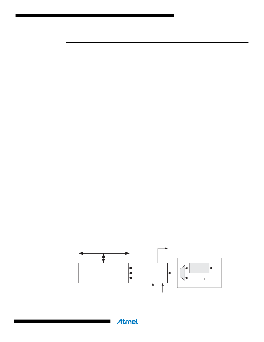
The main part of the 8-bit Timer/Counter is the programmable bi-directional counter unit. Figure
14-2 shows a block diagram of the counter and its surroundings.
Figure 14-2. Counter Unit Block Diagram
Signal description (internal signals):
Table 14-1.
Definitions
BOTTOM
The counter reaches the BOTTOM when it becomes 0x00.
MAX
The counter reaches its MAXimum when it becomes 0xFF (decimal 255).
TOP
The counter reaches the TOP when it becomes equal to the highest value in the
count sequence. The TOP value can be assigned to be the fixed value 0xFF
(MAX) or the value stored in the OCR0A Register. The assignment is depen-
dent on the mode of operation.
DATA BUS
TCNTn
Control Logic
count
TOVn
(Int.Req.)
Clock Select
top
Tn
Edge
Detector
( From Prescaler )
clk
Tn
bottom
direction
clear
相关PDF资料 |
PDF描述 |
|---|---|
| R5F3650NDFB | MICROCONTROLLER, PQFP100 |
| R5F3650RNFB | MICROCONTROLLER, PQFP100 |
| R5F3651ENFC | MICROCONTROLLER, PQFP128 |
| R5F3651KDFC | MICROCONTROLLER, PQFP128 |
| R5F21217KFP | 8-BIT, FLASH, 20 MHz, MICROCONTROLLER, PQFP48 |
相关代理商/技术参数 |
参数描述 |
|---|---|
| R5F3650MDFB#30 | 制造商:Renesas Electronics Corporation 功能描述:IC MCU 16BIT 512KB FLASH 100QFP 制造商:Renesas Electronics Corporation 功能描述:M16C Series 16 Bit 512 kB Flash 31 kB Ram SMT Microcontroller - LQFP-100 |
| R5F3650MDFB#U0 | 功能描述:MCU 4KB FLASH 512/16K 100-LQFP RoHS:是 类别:集成电路 (IC) >> 嵌入式 - 微控制器, 系列:M16C™ M16C/60/65 标准包装:96 系列:PIC® 16F 核心处理器:PIC 芯体尺寸:8-位 速度:20MHz 连通性:I²C,SPI 外围设备:欠压检测/复位,POR,PWM,WDT 输入/输出数:11 程序存储器容量:3.5KB(2K x 14) 程序存储器类型:闪存 EEPROM 大小:- RAM 容量:128 x 8 电压 - 电源 (Vcc/Vdd):2.3 V ~ 5.5 V 数据转换器:A/D 8x10b 振荡器型:内部 工作温度:-40°C ~ 125°C 封装/外壳:14-TSSOP(0.173",4.40mm 宽) 包装:管件 |
| R5F3650MDFB#V2 | 制造商:Renesas Electronics Corporation 功能描述:M16C65 FL 512/31 100QFP 2.7-5. 制造商:Renesas Electronics Corporation 功能描述:M16C65 FL 512/31 100QFP 2.7-5.5V -40/85C - Trays 制造商:Renesas Electronics Corporation 功能描述:MCU 32BIT 512KB FLASH 100QFP |
| R5F3650MNFA | 制造商:RENESAS 制造商全称:Renesas Technology Corp 功能描述:This MCU consumes low power, and supports operating modes |
| R5F3650MNFB | 制造商:RENESAS 制造商全称:Renesas Technology Corp 功能描述:This MCU consumes low power, and supports operating modes |
发布紧急采购,3分钟左右您将得到回复。