- 您现在的位置:买卖IC网 > PDF目录11679 > R5F562N8ADFP#V0 (Renesas Electronics America)MCU 32BIT FLASH 512KROM 100LQFP PDF资料下载
参数资料
| 型号: | R5F562N8ADFP#V0 |
| 厂商: | Renesas Electronics America |
| 文件页数: | 120/148页 |
| 文件大小: | 0K |
| 描述: | MCU 32BIT FLASH 512KROM 100LQFP |
| 产品培训模块: | RX Compare Match Timer RX DMAC |
| 标准包装: | 1 |
| 系列: | RX600 |
| 核心处理器: | RX |
| 芯体尺寸: | 32-位 |
| 速度: | 100MHz |
| 连通性: | EBI/EMI,I²C,SCI,SPI,USB |
| 外围设备: | DMA,LVD,POR,PWM,WDT |
| 输入/输出数: | 72 |
| 程序存储器容量: | 512KB(512K x 8) |
| 程序存储器类型: | 闪存 |
| RAM 容量: | 96K x 8 |
| 电压 - 电源 (Vcc/Vdd): | 2.7 V ~ 3.6 V |
| 数据转换器: | A/D 8x10/12b,D/A 1x10b |
| 振荡器型: | 内部 |
| 工作温度: | -40°C ~ 85°C |
| 封装/外壳: | 100-LQFP |
| 包装: | 托盘 |
第1页第2页第3页第4页第5页第6页第7页第8页第9页第10页第11页第12页第13页第14页第15页第16页第17页第18页第19页第20页第21页第22页第23页第24页第25页第26页第27页第28页第29页第30页第31页第32页第33页第34页第35页第36页第37页第38页第39页第40页第41页第42页第43页第44页第45页第46页第47页第48页第49页第50页第51页第52页第53页第54页第55页第56页第57页第58页第59页第60页第61页第62页第63页第64页第65页第66页第67页第68页第69页第70页第71页第72页第73页第74页第75页第76页第77页第78页第79页第80页第81页第82页第83页第84页第85页第86页第87页第88页第89页第90页第91页第92页第93页第94页第95页第96页第97页第98页第99页第100页第101页第102页第103页第104页第105页第106页第107页第108页第109页第110页第111页第112页第113页第114页第115页第116页第117页第118页第119页当前第120页第121页第122页第123页第124页第125页第126页第127页第128页第129页第130页第131页第132页第133页第134页第135页第136页第137页第138页第139页第140页第141页第142页第143页第144页第145页第146页第147页第148页
2004 Microchip Technology Inc.
DS39609B-page 71
PIC18F6520/8520/6620/8620/6720/8720
6.0
EXTERNAL MEMORY
INTERFACE
The External Memory Interface is a feature of the
PIC18F8X20 devices that allows the controller to
access external memory devices (such as Flash,
EPROM, SRAM, etc.) as program or data memory.
The physical implementation of the interface uses 27
pins. These pins are reserved for external address/data
bus functions; they are multiplexed with I/O port pins on
four ports. Three I/O ports are multiplexed with the
address/data bus, while the fourth port is multiplexed
with the bus control signals. The I/O port functions are
enabled when the EBDIS bit in the MEMCON register
is set (see Register 6-1). A list of the multiplexed pins
and their functions is provided in Table 6-1.
As implemented in the PIC18F8X20 devices, the
interface operates in a similar manner to the external
memory interface introduced on PIC18C601/801
microcontrollers. The most notable difference is that
the interface on PIC18F8X20 devices only operates in
16-bit modes. The 8-bit mode is not supported.
For a more complete discussion of the operating modes
that use the external memory interface, refer to
6.1
Program Memory Modes and the
External Memory Interface
As previously noted, PIC18F8X20 controllers are
capable of operating in any one of four program
memory modes, using combinations of on-chip and
external program memory. The functions of the multi-
plexed port pins depend on the program memory
mode selected, as well as the setting of the EBDIS bit.
In Microprocessor Mode, the external bus is always
active and the port pins have only the external bus
function.
In Microcontroller Mode, the bus is not active and
the pins have their port functions only. Writes to the
MEMCOM register are not permitted.
In Microprocessor with Boot Block or Extended
Microcontroller Mode, the external program memory
bus shares I/O port functions on the pins. When the
device is fetching or doing table read/table write
operations on the external program memory space, the
pins will have the external bus function. If the device is
fetching and accessing internal program memory loca-
tions only, the EBDIS control bit will change the pins
from external memory to I/O port functions. When
EBDIS = 0, the pins function as the external bus.
When EBDIS = 1, the pins function as I/O ports.
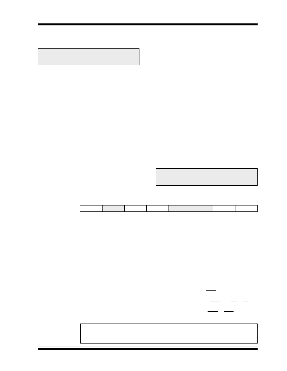
REGISTER 6-1:
MEMCON REGISTER
Note:
The External Memory Interface is not
implemented on PIC18F6X20 (64-pin)
devices.
Note:
Maximum FOSC for the PIC18FX520 is
limited to 25 MHz when using the external
memory interface.
R/W-0
U-0
R/W-0
U-0
R/W-0
EBDIS
—WAIT1
WAIT0
—
—WM1
WM0
bit7
bit0
bit 7
EBDIS: External Bus Disable bit
1
= External system bus disabled, all external bus drivers are mapped as I/O ports
0
= External system bus enabled and I/O ports are disabled
bit 6
Unimplemented: Read as ‘0’
bit 5-4
WAIT<1:0>: Table Reads and Writes Bus Cycle Wait Count bits
11
= Table reads and writes will wait 0 TCY
10
= Table reads and writes will wait 1 TCY
01
= Table reads and writes will wait 2 TCY
00
= Table reads and writes will wait 3 TCY
bit 3-2
Unimplemented: Read as ‘0’
bit 1-0
WM<1:0>: TBLWRT Operation with 16-bit Bus bits
1x
= Word Write mode: TABLAT<0> and TABLAT<1> word output, WRH active when
TABLAT<1> written
01
= Byte Select mode: TABLAT data copied on both MSB and LSB, WRH and (UB or LB)
will activate
00
= Byte Write mode: TABLAT data copied on both MSB and LSB, WRH or WRL will activate
Legend:
R = Readable bit
W = Writable bit
U = Unimplemented bit, read as ‘0’
- n = Value at POR
‘1’ = Bit is set
‘0’ = Bit is cleared
x = Bit is unknown
相关PDF资料 |
PDF描述 |
|---|---|
| VI-J3X-IZ-B1 | CONVERTER MOD DC/DC 5.2V 25W |
| VI-BVK-IX-F2 | CONVERTER MOD DC/DC 40V 75W |
| VI-J3X-IY-F3 | CONVERTER MOD DC/DC 5.2V 50W |
| VI-BVK-IX-F1 | CONVERTER MOD DC/DC 40V 75W |
| R5F56217BDBG#U0 | MCU 32BIT FLASH 384KROM 176LFBGA |
相关代理商/技术参数 |
参数描述 |
|---|---|
| R5F562N8ADLE | 制造商:Renesas Electronics Corporation 功能描述:MCU 32BIT RX62N 145LGA 制造商:Renesas Electronics Corporation 功能描述:MCU, 32BIT, RX62N, 145LGA 制造商:Renesas Electronics Corporation 功能描述:MCU, 32BIT, RX62N, 145LGA, Controller Family/Series:RX600, Core Size:32bit, No. of I/O's:103, Supply Voltage Min:2.7V, Supply Voltage Max:3.6V, Digital IC Case Style:LGA, No. of Pins:145, Program Memory Size:512KB, RAM Memory , RoHS Compliant: Yes |
| R5F562N8ADLE#U0 | 功能描述:MCU 32BIT FLASH 512KROM 145TFLGA RoHS:是 类别:集成电路 (IC) >> 嵌入式 - 微控制器, 系列:RX600 标准包装:1 系列:87C 核心处理器:MCS 51 芯体尺寸:8-位 速度:16MHz 连通性:SIO 外围设备:- 输入/输出数:32 程序存储器容量:8KB(8K x 8) 程序存储器类型:OTP EEPROM 大小:- RAM 容量:256 x 8 电压 - 电源 (Vcc/Vdd):4 V ~ 6 V 数据转换器:- 振荡器型:外部 工作温度:0°C ~ 70°C 封装/外壳:44-DIP 包装:管件 其它名称:864285 |
| R5F562N8BDBG | 制造商:Renesas Electronics Corporation 功能描述:MCU 32BIT RX62N 176BGA 制造商:Renesas Electronics Corporation 功能描述:MCU, 32BIT, RX62N, 176BGA 制造商:Renesas Electronics Corporation 功能描述:MCU, 32BIT, RX62N, 176BGA, Controller Family/Series:RX600, Core Size:32bit, No. of I/O's:126, Supply Voltage Min:2.7V, Supply Voltage Max:3.6V, Digital IC Case Style:LFBGA, No. of Pins:176, Program Memory Size:512KB, RAM Memory , RoHS Compliant: Yes |
| R5F562N8BDBG#U0 | 功能描述:MCU 32BIT FLASH 512K ROM 176BGA RoHS:是 类别:集成电路 (IC) >> 嵌入式 - 微控制器, 系列:RX600 标准包装:1 系列:87C 核心处理器:MCS 51 芯体尺寸:8-位 速度:16MHz 连通性:SIO 外围设备:- 输入/输出数:32 程序存储器容量:8KB(8K x 8) 程序存储器类型:OTP EEPROM 大小:- RAM 容量:256 x 8 电压 - 电源 (Vcc/Vdd):4 V ~ 6 V 数据转换器:- 振荡器型:外部 工作温度:0°C ~ 70°C 封装/外壳:44-DIP 包装:管件 其它名称:864285 |
| R5F562N8BDFB | 制造商:Renesas Electronics Corporation 功能描述:MCU 32BIT RX62N 144QFP |
发布紧急采购,3分钟左右您将得到回复。