- 您现在的位置:买卖IC网 > PDF目录230914 > RD-14592D1-545S (DATA DEVICE CORP) SYNCHRO OR RESOLVER TO DIGITAL CONVERTER, MDMA36 PDF资料下载
参数资料
| 型号: | RD-14592D1-545S |
| 厂商: | DATA DEVICE CORP |
| 元件分类: | 位置变换器 |
| 英文描述: | SYNCHRO OR RESOLVER TO DIGITAL CONVERTER, MDMA36 |
| 封装: | DDIP-36 |
| 文件页数: | 12/16页 |
| 文件大小: | 150K |
| 代理商: | RD-14592D1-545S |
5
Data Device Corporation
www.ddc-web.com
SD-14590/91/92
D-02/02-250
instance, a 1000 V transient can be generated when the primary
of a CX or TX driving a synchro or resolver input is opened. See
FIGURE 3.
FEEDBACK LOOP
The feedback loop produces a digital angle
φ which tracks the
analog input angle
θ to within the specified accuracy of the con-
verter. The control transformer performs the following trigono-
metric computation:
sin(
θ - φ) = sinθ cosφ - cosθ sinφ
where
θ is the angle representing the resolver shaft position, and
φ is the digital angle contained in the up/down counter. The track-
ing process consists of continually adjusting
φ to make (θ - φ) =
0, so that
φ will represent the shaft position θ. The output of the
demodulator is an analog DC level proportional to sin(
θ - φ). The
error processor receives its input from the demodulator and inte-
grates this sin(
θ - φ) error signal which then drives a Voltage
Controlled Oscillator (VCO). The VCO’s clock pulses are accu-
mulated by the up/down counter. The velocity voltage accuracy,
linearity and offset are determined by the quality of the VCO.
Functionally, the up/down counter is an incremental integrator.
Therefore, there are two stages of integration which make the
converter a Type II tracking servo. In a Type II servo, the VCO
always settles to a counting rate which makes d
φ/dt equal to
d
θ/dt without a lag. The output data will always be fresh and
available as long as the maximum tracking rate of the converter
is not exceeded.
SYNTHESIZED REFERENCE
The synthesized reference section of the SD-14590 eliminates
errors caused by quadrature voltage. Due to the inductive nature
of synchros and resolvers, their signals lead the reference signal
(RH and RL) by about 6°. When an uncompensated reference
signal is used to demodulate the control transformer’s output,
quadrature voltages are not completely eliminated. In a 14-bit
converter it is not necessary to compensate for the reference sig-
nal’s phase shift. A 6° phase shift will, however, cause problems
for the one minute accuracy converters. As shown in FIGURE 1,
the converter synthesizes its own cos(
ωt + α) reference signal
from the sin
θcos(ωt + α), cosθcos(ωt + α) signal inputs and from
the cos
ωt reference input. The phase angle of the synthesized
reference is determined by the signal input. The reference input
is used to choose between the +180° and -180° phases. The
synthesized reference will always be exactly in phase with the
signal input, and quadrature errors will therefore be eliminated.
The synthesized reference circuit also eliminates the 180° false
error null hangup.
Quadrature voltages in a resolver or synchro are by definition the
resulting 90° fundamental signal in the nulled out error voltage
(e) in the converter. A digital position error will result due to the
interaction of this quadrature voltage and a reference phase shift
between the converter signal and reference inputs. The magni-
tude of this error is given by the following formula:
Error = Quad/Full Scale (FS) signal * tan(
α)
Where: Error is in radians
Quad/FS signal is per unit quadrature input level.
α = signal to reference phase shift in degrees.
A typical example of the magnitude of this source of error is as
follows:
Quad/FS signal = .001
α = 6
Error = 0.35 min
≈1 LSB in the 16th bit.
Note: Quad/FS is composed of static quadrature which is specified by the
resolver or synchro supplier plus the speed voltage which is given by:
Speed Voltage = rotational speed/carrier frequency
Where: Speed Voltage is the per unit ratio of electrical
rotational speed in RPS divided by carrier frequency in Hz.
This error is totally negligible for 14-bit converters. For 16-bit con-
verters where the highest accuracy possible is needed and
where the quadrature and phase shift specifications can be high-
er, this source of error could be significant. The reference syn-
thesizer circuit in the converter which derives the reference from
the input signal essentially sets
α to zero resulting in complete
rejection of the quadrature.
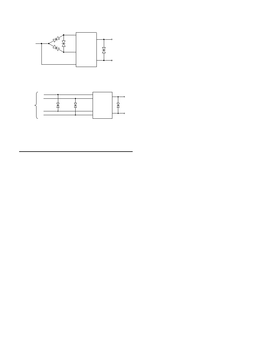
HYBRID
S3
S2
S1
RH
RL
CR1
CR2
S1
FOR 90 V SYNCHRO INPUTS
1N6071A
CR3
S2
S3
HYBRID
S3
S2
S1
S4
FOR 90 V RESOLVER INPUTS
CR4
CR5
S3
S2
S1
S4
90 V L-L
RESOLVER
INPUT
1N6071A
CR1, CR2, and CR3 are 1N6068A, bipolar transient voltage suppressors or
equivalent.
CR4 and CR5 are 1N6068A, bipolar transient voltage suppressors or equivalent.
FIGURE 3. CONNECTIONS FOR VOLTAGE
TRANSIENT SUPPRESSORS
相关PDF资料 |
PDF描述 |
|---|---|
| RD-14592D1-575 | SYNCHRO OR RESOLVER TO DIGITAL CONVERTER, MDMA36 |
| RD-14592F1-292 | SYNCHRO OR RESOLVER TO DIGITAL CONVERTER, CDMA36 |
| RD-14592F1-312Q | SYNCHRO OR RESOLVER TO DIGITAL CONVERTER, CDMA36 |
| RD-14592F1-315L | SYNCHRO OR RESOLVER TO DIGITAL CONVERTER, CDMA36 |
| RD-14591F1-172 | SYNCHRO OR RESOLVER TO DIGITAL CONVERTER, CDMA36 |
相关代理商/技术参数 |
参数描述 |
|---|---|
| RD-14595D1-102 | 制造商:未知厂家 制造商全称:未知厂家 功能描述:Resolver-to-Digital Converter |
| RD-14595D1-104 | 制造商:未知厂家 制造商全称:未知厂家 功能描述:Resolver-to-Digital Converter |
| RD-14595D1-105 | 制造商:未知厂家 制造商全称:未知厂家 功能描述:Resolver-to-Digital Converter |
| RD-14595D1-112 | 制造商:未知厂家 制造商全称:未知厂家 功能描述:Resolver-to-Digital Converter |
| RD-14595D1-114 | 制造商:未知厂家 制造商全称:未知厂家 功能描述:Resolver-to-Digital Converter |
发布紧急采购,3分钟左右您将得到回复。