- 您现在的位置:买卖IC网 > PDF目录230923 > RD-14596D1-322 (DATA DEVICE CORP) SYNCHRO OR RESOLVER TO DIGITAL CONVERTER, DIP36 PDF资料下载
参数资料
| 型号: | RD-14596D1-322 |
| 厂商: | DATA DEVICE CORP |
| 元件分类: | 位置变换器 |
| 英文描述: | SYNCHRO OR RESOLVER TO DIGITAL CONVERTER, DIP36 |
| 封装: | DDIP-36 |
| 文件页数: | 12/14页 |
| 文件大小: | 416K |
| 代理商: | RD-14596D1-322 |
INTERFACING - DIGITAL OUTPUTS AND CONTROLS
(CONTD)
DATA TRANSFERS
Digital output data from the SD-14595/96/97 can be transferred
to 8-bit and 16-bit bus systems. For 8-bit systems, the MSB and
LSB bytes are transferred sequentially. For 16-bit systems all
bits are transferred at the same time
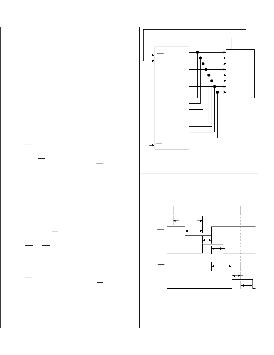
DATA TRANSFER TO 8-BIT BUS
FIGURES 11 and 12 show the connections and timing for trans-
ferring data from the SD-14595/96/97 to an 8-bit bus.
As can be seen by the timing diagram, the following occurs:
1. The converter INH control is applied and must remain low for
a minimum of 500 ns before valid data is transferred.
2. HBE is set to a low state (logic 0) 350 ns MIN after INH goes
low and must remain low for a minimum of 150 ns before the
MSB data (1-8) is valid and transferred.
3. As HBE is set to a high state (logic 1), LBE is brought low for
a 150 ns MIN before the LSB data is valid and transferred.
4. LBE should go high (to logic 1) at least 100 ns MAX before
another device uses the bus.
5.Setting INH high when data transfer is done, the data refresh
cycle can begin. Note the time it takes for INH to go to a logic 1
should be 100 ns minimum before valid data is transferred.
Note: For further understanding, refer to the beginning of this
section (Digital Interface, Digital Angle Outputs, Digital Angle
Output Timing, and Inhibit).
16-BIT DATA TRANSFER
Data transfer to the 16-bit bus is much simpler than the 8-bit bus.
FIGURES 13 and 14 (page 8) show the connections and timing
for transferring data from the SD-14595/96/97 to a 16-bit bus.
As can be seen by the timing diagram the following occurs:
1. The converter INH control is applied and must remain low for
a minimum of 500 ns before valid data is transferred.
2. HBE and LBE are set to a low state (logic 0) 350 ns MIN after
INH goes low and must remain low for a minimum of 150 ns
before the data (1-16) is valid and transferred.
3. HBE and LBE should go high (to logic 1) at least 100 ns MAX
before another device uses the bus.
4. INH goes high and data transfer is done and the data refresh
cycle can begin. Note the time it takes for INH to go to a logic 1
should be 100 ns minimum before valid data is transferred.
Note: For further understanding, refer to the beginning of this
section (Digital Interface, Digital Angle Outputs, Digital Angle
Output Timing, and Inhibit).
7
SD-14595/96/97
8-BIT BUS
(MSB) BIT 1
BIT 2
BIT 3
BIT 4
BIT 5
BIT 6
BIT 7
BIT 8
BIT 9
BIT 10
BIT 11
BIT 12
BIT 13
BIT 14
BIT 15
(LSB) BIT 16
D7
D6
D5
D4
D3
D2
D1
D0
HBE
LBE
INH
DATA 1-8
VALID
DATA 9-16
VALID
500 ns MIN
150 ns MIN
0 ns MIN
100 ns MAX
150 ns MIN
0 ns MIN
100 ns MAX
LBE
HBE
FIGURE 11. DATA TRANSFER TO 8-BIT BUS
FIGURE 12. DATA TRANSFER TO 8-BIT BUS TIMING
相关PDF资料 |
PDF描述 |
|---|---|
| RD-14597F2-804 | SYNCHRO OR RESOLVER TO DIGITAL CONVERTER, CDFP36 |
| RD-14597F3-124 | SYNCHRO OR RESOLVER TO DIGITAL CONVERTER, CDFP36 |
| RDC-19222-302K | SYNCHRO OR RESOLVER TO DIGITAL CONVERTER, PQCC44 |
| RDC-19222-303Q | SYNCHRO OR RESOLVER TO DIGITAL CONVERTER, PQCC44 |
| RD570-22HB | SYNCHRO OR RESOLVER TO DIGITAL CONVERTER, XMA42 |
相关代理商/技术参数 |
参数描述 |
|---|---|
| RD-14596F1-102 | 制造商:未知厂家 制造商全称:未知厂家 功能描述:Resolver-to-Digital Converter |
| RD-14596F1-104 | 制造商:未知厂家 制造商全称:未知厂家 功能描述:Resolver-to-Digital Converter |
| RD-14596F1-112 | 制造商:未知厂家 制造商全称:未知厂家 功能描述:Resolver-to-Digital Converter |
| RD-14596F1-114 | 制造商:未知厂家 制造商全称:未知厂家 功能描述:Resolver-to-Digital Converter |
| RD-14596F1-122 | 制造商:未知厂家 制造商全称:未知厂家 功能描述:Resolver-to-Digital Converter |
发布紧急采购,3分钟左右您将得到回复。