- 您现在的位置:买卖IC网 > PDF目录66126 > RD74LVC1G17WPE LVC/LCX/Z SERIES, 1-INPUT NON-INVERT GATE, PBGA5 PDF资料下载
参数资料
| 型号: | RD74LVC1G17WPE |
| 元件分类: | 门电路 |
| 英文描述: | LVC/LCX/Z SERIES, 1-INPUT NON-INVERT GATE, PBGA5 |
| 封装: | 0.70 X 1.10 MM, 0.40 MM HEIGHT, 0.40 MM PITCH, FBGA-5 |
| 文件页数: | 1/8页 |
| 文件大小: | 2154K |
| 代理商: | RD74LVC1G17WPE |
Rev.1.00 Feb 23, 2006 page 1 of 7
RD74LVC1G17
Schmitt-trigger Buffer
REJ03D0722–0100
Rev.1.00
Feb 23, 2006
Description
The RD74LVC1G17 has a Schmitt-trigger buffer in a 5-pin package. Low voltage and high-speed operation is suitable
for the battery powered products (e.g., notebook computers), and the low power consumption extends the battery life.
Features
The basic gate function is lined up as Renesas uni logic series.
Supply voltage range : 1.65 to 5.5 V
Operating temperature range: –40 to +85°C
All inputs:
VIH (Max.) = 5.5 V (@VCC = 0 V to 5.5 V)
All outputs: V
O (Max.) = 5.5 V (@VCC = 0 V)
Output current:
±4 mA (@VCC = 1.65 V)
±8 mA (@VCC = 2.3 V)
±24 mA (@VCC = 3.0 V)
±32 mA (@VCC = 4.5 V)
Ordering Information
Part Name
Package Type
Package Code
(Previous Code)
Package
Abbreviation
Taping Abbreviation
(Quantity)
RD74LVC1G17WPE
WCSP-5 pin
SXBG0005LB–A
(TBS-5CV)
WP
E (3,000 pcs/reel)
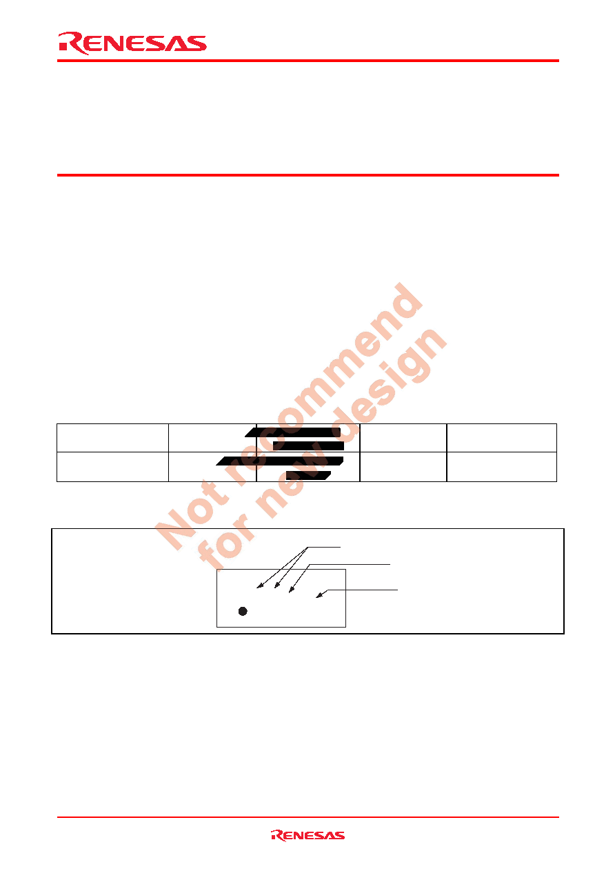
Article Indication
E K Y M
Marking
Year code
Month code
相关PDF资料 |
PDF描述 |
|---|---|
| RD74LVC1G240WPE | LVC/LCX/Z SERIES, 1-INPUT INVERT GATE, BGA5 |
| RD74LVC1G97WPE | SPECIALTY LOGIC CIRCUIT, PBGA6 |
| RD74LVC245BTELL | LVC/LCX/Z SERIES, 8-BIT TRANSCEIVER, TRUE OUTPUT, PDSO20 |
| RD74LVC273BTELL | LVC/LCX/Z SERIES, POSITIVE EDGE TRIGGERED D FLIP-FLOP, TRUE OUTPUT, PDSO20 |
| RD74LVC2G02WPE | LVC/LCX/Z SERIES, DUAL 2-INPUT NOR GATE, BGA8 |
相关代理商/技术参数 |
参数描述 |
|---|---|
| RD74LVC1G240 | 制造商:RENESAS 制造商全称:Renesas Technology Corp 功能描述:Bus Buffer Inverted with 3-state Output |
| RD74LVC1G240WPE | 制造商:RENESAS 制造商全称:Renesas Technology Corp 功能描述:Bus Buffer Inverted with 3-state Output |
| RD74LVC1G32 | 制造商:RENESAS 制造商全称:Renesas Technology Corp 功能描述:2-input OR Gate |
| RD74LVC1G32WPE | 制造商:RENESAS 制造商全称:Renesas Technology Corp 功能描述:2-input OR Gate |
| RD74LVC1G79 | 制造商:RENESAS 制造商全称:Renesas Technology Corp 功能描述:Single Positive Edge-triggered D-type Flip Flop |
发布紧急采购,3分钟左右您将得到回复。