- 您现在的位置:买卖IC网 > PDF目录378128 > RDA012M4MS-DI (Electronic Theatre Controls, Inc.) 12 Bit 1.3 GS/s Master-Slave 4:1 MUXDAC PDF资料下载
参数资料
| 型号: | RDA012M4MS-DI |
| 厂商: | Electronic Theatre Controls, Inc. |
| 英文描述: | 12 Bit 1.3 GS/s Master-Slave 4:1 MUXDAC |
| 中文描述: | 12位1.3 GS / s的主从4:1 MUXDAC |
| 文件页数: | 7/13页 |
| 文件大小: | 427K |
| 代理商: | RDA012M4MS-DI |
RDA012M4MS DATASHEET
DS_0017PB0-2805
Rockwell Scientific reserves the right to make changes to its product specifications at any time without notice.
The information furnished herein is believed to be accurate; however, no responsibility is assumed for its use.
Page 7 of 13
Theory of Operation
For best dynamic and static performance, the
DAC employs 6-bit segmentation. The 3.3V
NMOS compatible 12-bit digital data inputs are
latched by a master-slave flip-flop immediately
after the input buffer to reduce the data skew.
The four-channel data are combined together by
the 48:12 MUX and latched again. The 6 MSB
data bits are decoded into thermometer code by
a two-stage decoding block, and the 6 LSB data
bits are transported through the delay equalizer
block. The digital data are synchronized again
by a second master slave flip-flop to reduce the
switching glitch. The decoded 6 MSB data drive
63 identical current switches, and the 6 LSB
data drive 6 current switches. The output nodes
from the LSB current switches are connected to
the analog output through an R-2R ladder to
generate the binary output.
The DAC output full-scale voltage follows the
relationship V
FS
= 0.3xV
REF.
An internal
reference circuit with approximately -10dB
supply rejection is integrated on chip for
application convenience. The reference pin is
provided
for
monitoring
purposes. To band-limit the noise on the
reference voltage, the reference pin should be
bypassed to the GNDA node with capacitance >
100pF. The VREF pin can also be used to
override the internal reference with an accurate,
and
for
bypass
temperature-compensated
reference.
external
voltage
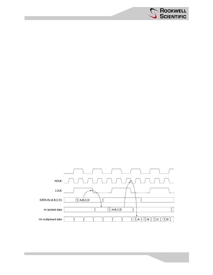
The timing diagram is shown in figure 3. The
1.3GHz external clock (HCLK) is divided by 2
and 4 resulting in the MUX internal selection
signals S0 and S1. A low-speed clock (LCLK) is
provided to drive the external digital. The four-
channel data input are latched with an internal
clock that is synchronized with the LCLK.
Controlled by S0 and S1, input data are fed to
the 1.3GS/s DAC in the order shown.
For applications requiring two MUXDACs, such
as quadrature modulation, the RDA012M4MS
offers master and slave mode operation. This
provides synchronization between the two
MUXDACs in a straightforward manner. Figure 4
illustrates two MUXDACs in an I-Q configuration
and 1 GS/s conversion rate. The I-MUXDAC is
in master mode and the Q-MUXDAC is in slave
mode. The master MUXDAC generates an
LVDS compatible 250MHz clock signal that is
input to the slave MUXDAC were it is used to
synchronize the generation of the select signal
for the input muxes. The slave device then feeds
this clock to the FPGA clock driver. For proper
synchronization, the delay associated with the
LVDS clock signal from master to slave
MUXDAC must not exceed one clock period of
the high-speed clock.
Figure 4 - Input Timing Diagram.
相关PDF资料 |
PDF描述 |
|---|---|
| RDA012M4MS-HD | 12 Bit 1.3 GS/s Master-Slave 4:1 MUXDAC |
| RDA012M4 | 12 Bit 1.3 GS/s 4:1 MUXDAC |
| RDA012M4-DI | 12 Bit 1.3 GS/s 4:1 MUXDAC |
| RDA012M4-HD | 12 Bit 1.3 GS/s 4:1 MUXDAC |
| RDL60V | RESETABLE FUSES |
相关代理商/技术参数 |
参数描述 |
|---|---|
| RDA012M4MS-HD | 制造商:未知厂家 制造商全称:未知厂家 功能描述:12 Bit 1.3 GS/s Master-Slave 4:1 MUXDAC |
| RDA1005LTR7 | 制造商:RF Micro Devices Inc 功能描述:IC AMP DVGA 32-MCM 5.2X5.2 |
| RDA-125BAG1A | 功能描述:以太网和电信连接器 RJ-45 W/ TRANSFORMER CONNECTOR/UDE RoHS:否 制造商:Pulse 产品:Modular Jacks 性能类别: USOC 代码:RJ45 位置/触点数量: 安装风格:Through Hole 端口数量:1 x 1 型式:Female 屏蔽: 电流额定值: 电压额定值: 触点电镀: 外壳材料:Thermoplastic IP 等级: |
| RDA1U4 | 功能描述:机架和机柜配件 RoHS:否 制造商:Bivar 产品:Rack Accessories 面板空间: 颜色:Black |
| RDA2U4 | 功能描述:机架和机柜配件 RoHS:否 制造商:Bivar 产品:Rack Accessories 面板空间: 颜色:Black |
发布紧急采购,3分钟左右您将得到回复。