- 您现在的位置:买卖IC网 > PDF目录230922 > RDC-19220S-422K (DATA DEVICE CORP) SYNCHRO OR RESOLVER TO DIGITAL CONVERTER, CDIP40 PDF资料下载
参数资料
| 型号: | RDC-19220S-422K |
| 厂商: | DATA DEVICE CORP |
| 元件分类: | 位置变换器 |
| 英文描述: | SYNCHRO OR RESOLVER TO DIGITAL CONVERTER, CDIP40 |
| 封装: | 2 X 0.600 INCH, 0.200 INCH HEIGHT, CERAMIC, DDIP-40 |
| 文件页数: | 14/20页 |
| 文件大小: | 276K |
| 代理商: | RDC-19220S-422K |
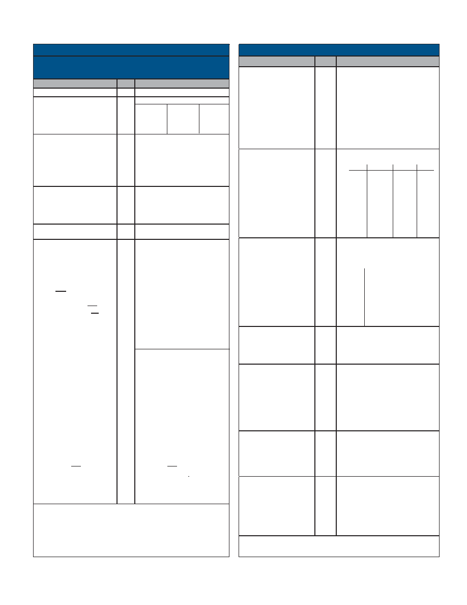
3
Data Device Corporation
www.ddc-web.com
RDC-19220/2S
E-11/02-300
These specifications apply over the rated power supply, tempera-
ture, and reference frequency ranges; 15% signal amplitude varia-
tion & 10% harmonic distortion.
PARAMETER
VALUE
UNIT
RESOLUTION
10, 12, 14, or 16 (notes 1 & 2)
Bits
REFERENCE
Type
Voltage: differential
single ended
overload
Frequency
Input Impedance
(+REF, -REF)
Differential
±10 max
±5 max
±25 continuous 100 transient
DC to 10,000
10M min //20 pf
V
Hz
Ohm
SIGNAL INPUT
Type
Voltage: operating
overload
Input Impedance
(+S, -S, SIN, +C, -C, COS)
Resolver, differential, groundbased
2 ±15%
±25 continuous
10M min //10 pf.
Vrms
V
Ohm
REFERENCE
±Sig/Ref Phase Shift
(note 5)
45 max from 400 Hz to 10 kHz
deg
DIGITAL INPUT/OUTPUT
Logic Type
Inputs
Inhibit (INH)
Enable Bits 1 to 8 (EM)
Enable Bits 9 to 16 (EL)
Resolution and Mode
Control (A & B)
(see notes 1 and 2)
Outputs
Parallel Data (1-16)
Converter Busy (CB)
Built-in-Test (BIT)
TTL/CMOS compatible
Logic 0 = 0.8 V max.
Logic 1 = 2.0 V min.
Loading=10 A max P.U. current
source to +5 V //5 pF max.
CMOS transient protected
Logic 0 inhibits; Data stable
within 0.1 S
Logic 0 enables; Data stable
within 150 nS
Logic 1 = High Impedance
Data High Z within 100 nS
Mode
B
A
Resolution
Resolver
0
10 bits
“
0
1
12 bits
“
1
0
14 bits
“
1
16 bits
LVDT
-5 V
0
8 bits
“
0
-5 V
10 bits
“
1
-5 V
12 bits
“
-5 V -5 V
14 bits
10, 12, 14 or 16 parallel lines;
natural binary angle positive
logic (see note 2)
0.25 to 0.75 s positive pulse
leading edge initiates counter
update.
Logic 0 for BIT condition.
±100 LSBs of error with a filter of
500 S total, Loss-of-Signal (LOS)
less than 500 mV, or Loss-of-
Reference (LOR) less than 500 mV.
PARAMETER
VALUE
UNIT
TABLE 1. RDC-19220/2S SPECIFICATIONS (CONT.)
DIGITAL INPUT/OUTPUT
Outputs (continued)
Drive Capability
50 pF+
Logic 0; 1 TTL load, 1.6 mA at
0.4 V max.
Logic 1; 10 TTL loads, -0.4 mA
at 2.8 V min
Logic 0; 100 mV max driving CMOS
Logic 1; +5 V supply minus 100 mV
min driving CMOS High Z; 10 uA //5
pF max
DYNAMIC
CHARACTERISTICS
Resolution
Tracking Rate-min(note 6)
Bandwidth(Closed Loop) Max
Ka
A1
A2
A
B
Acceleration (1 LSB lag)
Settling Time(179° step)
bits
rps
Hz
1/sec2
1/sec
deg/s2
msec
(at maximum bandwidth)
10
12
14
16
1152
288
72
18
1200
600
300
5.7M
1.4M
360k
19.5
4.9
1.2
295k
2400
1200
600
1200
600
300
2M
500k
30k
2k
2
8
20
50
VELOCITY
CHARACTERISTICS
Polarity
Voltage Range(Full Scale)
Scale Factor Error
Scale Factor TC
Reversal Error
Linearity
Zero Offset
Zero Offset TC
Load
Noise
V
%
PPM/C
%
mV
V/C
k
Vp/V
Positive for increasing angle
±4 (at nominal ps)
10 typ
20 max
100 typ
200 max
0.75 typ
1.3 max
0.25 typ
0.50 max
5 typ
10 max
15 typ
30 max
8 max
1 typ
0.125 min, 2 max
POWER SUPPLIES
Nominal Voltage
Voltage Range
Max Volt. w/o Damage
Current
V
%
V
mA
(note 6 and 7)
+5
-5
±5
+7
-7
14 typ, 22 max (each)
TEMPERATURE RANGE
Operating
-30X
-20X
-10X
Storage
-30X or -20X
-10X
°C
0 to +70
-40 to +85
-55 to +125
-65 to +150
PHYSICAL
CHARACTERISTICS
Size: 40-pin DDIP
44-pin J-lead
Weight:
40-pin DDIP
44-pin J-lead
in(mm)
oz (g)
2.0 x 0.6 x 0.2 (50.8 x 15.24 x 5.08)
0.690 square (17.526)
Plastic
Ceramic
0.21 (5.95)
0.24 (6.80)
0.08 (2.27)
0.064 (1.84)
FREQUENCY RANGE
ACCURACY -XX2
-XX3 (NOTE 3)
REPEATABILITY
DIFFERENTIAL LINEARITY
Hz
Min
LSB
47-1k(note 4) 1k - 4k
4k - 10k
4 +1 LSB
4 +1 LSB 5 +1 LSB
2 +1 LSB
2 +1 LSB 3 +1 LSB
± 1
± 2
± 1
± 2
TABLE 1. RDC-19220/2S SPECIFICATIONS
Notes: 6. See text, General Setup Considerations.
(cont.)
7. When using internally generated -5V the internal -5V charge pump
when measured at the converter pin, may be as low as -20% (or -4V).
Notes: 1. Unused data bits are set to logic “0.”
2. In LVDT mode, bit 16 is LSB for 14-bit resolution or bit 12 is
LSB for 10-bit resolution
3. Accuracy in LVDT mode is 0.15% + 1 LSB of full scale.
4. If the frequency is between 47Hz and 1kHz, then there may
be 1 LSB of jitter at quadrant boundaries.
5. The maximum phase shift tolerance will degrade linearly
from 45 degrees at 400 Hz to 30 degrees at 60 Hz.
THERMAL RESISTANCE
Junction to Case,
θjc
40 Pin DDIP (Plastic)
40 Pin DDIP (Ceramic)
44 Pin J-Lead (Plastic)
44 Pin J-Lead (Ceramic)
°C/W
92.4
4.6
72.6
2.4
相关PDF资料 |
PDF描述 |
|---|---|
| RDC-19220S-422L | SYNCHRO OR RESOLVER TO DIGITAL CONVERTER, CDIP40 |
| RD-14597F1-234L | SYNCHRO OR RESOLVER TO DIGITAL CONVERTER, CDFP36 |
| RD-14591D1-434 | SYNCHRO OR RESOLVER TO DIGITAL CONVERTER, MDMA36 |
| RDC-19223-122 | SYNCHRO OR RESOLVER TO DIGITAL CONVERTER, CDIP40 |
| RDC-19221-201 | SYNCHRO OR RESOLVER TO DIGITAL CONVERTER, PDIP28 |
相关代理商/技术参数 |
参数描述 |
|---|---|
| RDC19221-101 | 制造商:未知厂家 制造商全称:未知厂家 功能描述:Converter IC |
| RDC-19221-102 | 制造商:未知厂家 制造商全称:未知厂家 功能描述:LVDT/Resolver-to-Digital Converter |
| RDC-19221-103 | 制造商:未知厂家 制造商全称:未知厂家 功能描述:LVDT/Resolver-to-Digital Converter |
| RDC19221-121 | 制造商:未知厂家 制造商全称:未知厂家 功能描述:Converter IC |
| RDC-19221-122 | 制造商:未知厂家 制造商全称:未知厂家 功能描述:LVDT/Resolver-to-Digital Converter |
发布紧急采购,3分钟左右您将得到回复。