- 您现在的位置:买卖IC网 > PDF目录230923 > RDC-19224-A03 (DATA DEVICE CORP) SYNCHRO OR RESOLVER TO DIGITAL CONVERTER, PQFP44 PDF资料下载
参数资料
| 型号: | RDC-19224-A03 |
| 厂商: | DATA DEVICE CORP |
| 元件分类: | 位置变换器 |
| 英文描述: | SYNCHRO OR RESOLVER TO DIGITAL CONVERTER, PQFP44 |
| 封装: | PLASTIC, MQFP-44 |
| 文件页数: | 3/24页 |
| 文件大小: | 1233K |
| 代理商: | RDC-19224-A03 |
11
Data Device Corporation
www.ddc-web.com
RDC-19220 SERIES
V-12/08-0
R i
S1
S3
+S
-S
SIN
Rf
R i
Rf
R i
S4
S2
+C
-C
Rf
R i
Rf
COS
A GND
CONVERTER
8 10
-
+
-
+
RESOLVER
INPUT
R i
S1
S3
+S
-S
SIN
Rf
R i
Rf
R i
S4
S2
+C
-C
Rf
R i
Rf
COS
A GND
CONVERTER
8 10
12
15
13
2
3
1
6
16
7
4
5
-
+
-
+
RESOLVER
INPUT
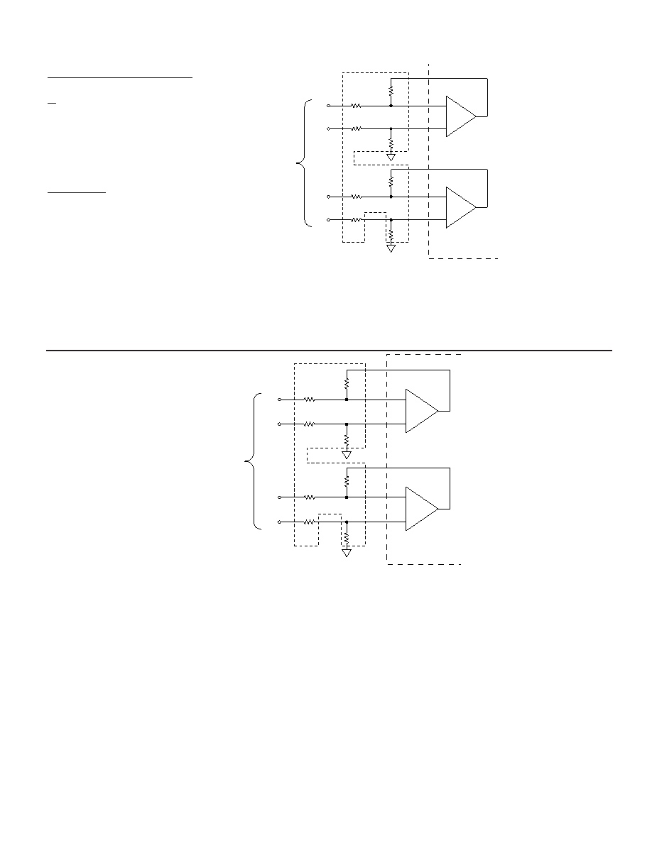
Notes:
1) S1 and S3, S2 and S4, and RH and RL should be ideally twisted shielded, with the shield tied to gND at the converter.
2) For 2V direct input use 10k matched resistors for Ri & Rf.
Examples of Component Calculations:
Component Formula
Ri x 2 Vrms = Resolver L-L rms voltage
Rf
Rf ≥ 6 k
1) 2V in, need gain of 1, use 10k for Rf and Ri
gain = Rf/Ri
2) 4V in, need gain of 0.5, Rf = 10k, Ri = 20k
To calculate Ri:
Select 10k for Rf
Ri = Rf x 0.5 x (input L-L volt)
Ri = 10k x 0.5 x (input L-L volt)
FIGURE 8A. dIFFERENTIAL REsOLVER INPUT
FIGURE 8B. dIFFERENTIAL REsOLVER INPUT, UsING ddc-49530, ddc-57470 (11.8 V),
ddc-73089 (2V), OR ddc-49590 (90 V)
1) S1 and S3, S2 and S4, and RH and RL should be ideally twisted shielded, with the shield tied to gND at the converter.
2) For DDC-49530 or DDC-57470: Ri = 70.8 k
, 11.8 V input, synchro or resolver. For DDC-49590: Ri = 270 k, 90 V input, synchro or resolver.
3) Maximum additional error is 1 LSB using recommended thin film package.
4) Note on dc Offset Gains: Input options affect DC offset gains and therefore affect carrier frequency ripple and jitter. Offsets gains associated with differ-
ential mode, (offset gain for differential configuration = 1 + RF/RI) and direct mode (offset gain for direct configuration = 1), show differential will always be
higher. Higher DC offsets cause higher carrier frequency ripple due to demodulation process. This carrier frequency ripple because it is riding on the top of
the DC error signal causes jitter. A higher carrier frequency vs bandwidth ratio will help decrease ripple and jitter associated with offsets. Summary: R/D’s with
differential inputs are more susceptible to offset problems than R/D’s in single ended mode. RD’s in higher resolutions, such as 16 bit, will further compound
offset issues due to higher internal voltage gains. Although the differential configuration has a higher DC offset gain, the differential configuration’s common
mode noise rejection makes it the preferred input option. The tradeoffs should be considered on a design to design basis. Also refer to FAQ-gIQ-021.
相关PDF资料 |
PDF描述 |
|---|---|
| RDC-634-H-3-A | SYNCHRO OR RESOLVER TO DIGITAL CONVERTER, DMA27 |
| RDC-632-M-1 | SYNCHRO OR RESOLVER TO DIGITAL CONVERTER, DMA27 |
| RDC-19229S-483Z | SYNCHRO OR RESOLVER TO DIGITAL CONVERTER, CQCC40 |
| RDC-19229-422L | SYNCHRO OR RESOLVER TO DIGITAL CONVERTER, CQCC44 |
| RD-14595D1-382Z | SYNCHRO OR RESOLVER TO DIGITAL CONVERTER, DIP36 |
相关代理商/技术参数 |
参数描述 |
|---|---|
| RDC20-100M-RC | 制造商:ALLIED 制造商全称:Allied Components International 功能描述:Radial Drum Core Inductors |
| RDC20-101K-RC | 制造商:ALLIED 制造商全称:Allied Components International 功能描述:Radial Drum Core Inductors |
| RDC20-102K-RC | 制造商:ALLIED 制造商全称:Allied Components International 功能描述:Radial Drum Core Inductors |
| RDC20110D05 | 功能描述:DC/DC CONVERTER +/-5V 20W 制造商:xp power 系列:RDC 包装:管件 零件状态:有效 类型:隔离模块 输出数:2 电压 - 输入(最小值):55V 电压 - 输入(最大值):176V 电压 - 输出 1:5V 电压 - 输出 2:-5V 电压 - 输出 3:- 电流 - 输出(最大值):2A,2A 功率(W) - 制造系列:20W 电压 - 隔离:1.5kV(1500V) 应用:轨道 特性:远程开/关,OCP,OTP,OVP,SCP,UVLO 安装类型:通孔 封装/外壳:6-DIP 模块 大小/尺寸:2.00" 长 x 1.00" 宽 x 0.42" 高(50.8mm x 25.4mm x 10.6mm) 工作温度:-40°C ~ 85°C 效率:86% 功率(W) - 最大值:20W 标准包装:10 |
| RDC20110D12 | 功能描述:DC/DC CONVERTER +/-12V 20W 制造商:xp power 系列:RDC 包装:管件 零件状态:有效 类型:隔离模块 输出数:2 电压 - 输入(最小值):55V 电压 - 输入(最大值):176V 电压 - 输出 1:12V 电压 - 输出 2:-12V 电压 - 输出 3:- 电流 - 输出(最大值):830mA,830mA 功率(W) - 制造系列:20W 电压 - 隔离:1.5kV(1500V) 应用:轨道 特性:远程开/关,OCP,OTP,OVP,SCP,UVLO 安装类型:通孔 封装/外壳:6-DIP 模块 大小/尺寸:2.00" 长 x 1.00" 宽 x 0.42" 高(50.8mm x 25.4mm x 10.6mm) 工作温度:-40°C ~ 85°C 效率:84% 功率(W) - 最大值:20W 标准包装:10 |
发布紧急采购,3分钟左右您将得到回复。