- 您现在的位置:买卖IC网 > PDF目录17093 > REF191ESZ-REEL (Analog Devices Inc)IC VREF SERIES PREC 2.048V 8SOIC PDF资料下载
参数资料
| 型号: | REF191ESZ-REEL |
| 厂商: | Analog Devices Inc |
| 文件页数: | 20/28页 |
| 文件大小: | 0K |
| 描述: | IC VREF SERIES PREC 2.048V 8SOIC |
| 标准包装: | 2,500 |
| 系列: | REF19 |
| 基准类型: | 串联,精度 |
| 输出电压: | 2.048V |
| 容差: | ±2mV |
| 温度系数: | 5ppm/°C |
| 输入电压: | 2.3 V ~ 15 V |
| 通道数: | 1 |
| 电流 - 静态: | 15µA |
| 电流 - 输出: | 30mA |
| 工作温度: | -40°C ~ 85°C |
| 安装类型: | 表面贴装 |
| 封装/外壳: | 8-SOIC(0.154",3.90mm 宽) |
| 供应商设备封装: | 8-SO |
| 包装: | 带卷 (TR) |
第1页第2页第3页第4页第5页第6页第7页第8页第9页第10页第11页第12页第13页第14页第15页第16页第17页第18页第19页当前第20页第21页第22页第23页第24页第25页第26页第27页第28页
�� ��
��
��REF19x� Series�
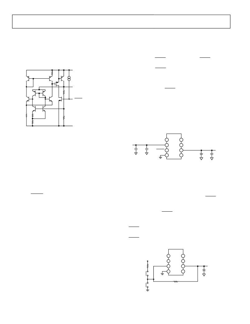
�APPLICATIONS� INFORMATION�
�OUTPUT� SHORT-CIRCUIT� BEHAVIOR�
�The� REF19x� family� of� devices� is� totally� protected� from� damage�
�due� to� accidental� output� shorts� to� GND� or� to� V� S� .� In� the� event� of�
�an� accidental� short-circuit� condition,� the� reference� device� shuts�
�down� and� limits� its� supply� current� to� 40� mA.�
�V� S�
�OUTPUT�
�SLEEP� (SHUTDOWN)�
�GND�
�Figure� 20.� Simplified� Schematic�
�Data� Sheet�
�SLEEP� MODE� OPERATION�
�All� REF19x� devices� include� a� sleep� capability� that� is� TTL/CMOS-�
�level� compatible.� Internally,� a� pull-up� current� source� to� V� S� is�
�connected� at� the� SLEEP� pin.� This� permits� the� SLEEP� pin� to� be�
�driven� from� an� open� collector/drain� driver.� A� logic� low� or� a� 0� V�
�condition� on� the� SLEEP� pin� is� required� to� turn� off� the� output�
�stage.� During� sleep,� the� output� of� the� references� becomes� a� high�
�impedance� state� where� its� potential� would� then� be� determined�
�by� external� circuitry.� If� the� sleep� feature� is� not� used,� it� is�
�recommended� that� the� SLEEP� pin� be� connected� to� V� S� (Pin� 2).�
�BASIC� VOLTAGE� REFERENCE� CONNECTIONS�
�The� circuit� in� Figure� 21� illustrates� the� basic� configuration� for�
�the� REF19x� family� of� references.� Note� the� 10� μF/0.1� μF� bypass�
�network� on� the� input� and� the� 1� μF/0.1� μF� bypass� network� on�
�the� output.� It� is� recommended� that� no� connections� be� made� to�
�Pin� 1,� Pin� 5,� Pin� 7,� and� Pin� 8.� If� the� sleep� feature� is� not� required,�
�Pin� 3� should� be� connected� to� V� S� .�
�DEVICE� POWER� DISSIPATION� CONSIDERATIONS�
�NC� 1�
�REF19x�
�8�
�NC�
�The� REF19x� family� of� references� is� capable� of� delivering� load�
�V� S�
�2�
�7�
�NC�
�NC�
�1μF� 0.1μF�
�currents� to� 30� mA� with� an� input� voltage� that� ranges� from� 3.3� V�
�to� 15� V.� When� these� devices� are� used� in� applications� with� large�
�input� voltages,� exercise� care� to� avoid� exceeding� the� maximum�
�internal� power� dissipation� of� these� devices.� Exceeding� the�
�published� specifications� for� maximum� power� dissipation� or�
�junction� temperature� can� result� in� premature� device� failure.�
�The� following� formula� should� be� used� to� calculate� the� maximum�
�junction� temperature� or� dissipation� of� the� device:�
�10μF� 0.1μF� OUTPUT�
�SLEEP� 3� 6�
�+�
�4� 5�
�TANT�
�NC� =� NO� CONNECT�
�Figure� 21.� Basic� Voltage� Reference� Connections�
�MEMBRANE� SWITCH-CONTROLLED� POWER� SUPPLY�
�With� output� load� currents� in� the� tens� of� mA,� the� REF19x� family� of�
�references� can� operate� as� a� low� dropout� power� supply� in� hand-held�
�P� D� =�
�T� J� ?� T� A�
�θ� JA�
�instrument� applications.� In� the� circuit� shown� in� Figure� 22,� a�
�membrane� on/off� switch� is� used� to� control� the� operation� of� the�
�reference.� During� an� initial� power-on� condition,� the� SLEEP� pin� is�
�where� T� J� and� T� A� are� the� junction� and� ambient� temperatures,�
�respectively;� P� D� is� the� device� power� dissipation;� and� θ� JA� is� the�
�device� package� thermal� resistance.�
�OUTPUT� VOLTAGE� BYPASSING�
�For� stable� operation,� low� dropout� voltage� regulators� and� references�
�generally� require� a� bypass� capacitor� connected� from� their� V� OUT�
�pins� to� their� GND� pins.� Although� the� REF19x� family� of� references� is�
�capable� of� stable� operation� with� capacitive� loads� exceeding� 100� μF,�
�a� 1� μF� capacitor� is� sufficient� to� guarantee� rated� performance.�
�The� addition� of� a� 0.1� μF� ceramic� capacitor� in� parallel� with� the�
�held� to� GND� by� the� 10� k� resistor.� Recall� that� this� condition� (read:�
�three-state)� disables� the� REF19x� output.� When� the� membrane� on�
�switch� is� pressed,� the� SLEEP� pin� is� momentarily� pulled� to� V� S� ,�
�enabling� the� REF19x� output.� At� this� point,� current� through� the� 10� k�
�resistor� is� reduced� and� the� internal� current� source� connected� to� the�
�SLEEP� pin� takes� control.� Pin� 3� assumes� and� remains� at� the� same�
�potential� as� V� S� .� When� the� membrane� off� switch� is� pressed,� the�
�SLEEP� pin� is� momentarily� connected� to� GND,� which� once�
�again� disables� the� REF19x� output.�
�REF19x�
�bypass� capacitor� improves� load� current� transient� performance.�
�For� best� line� voltage� transient� performance,� it� is� recommended�
�that� the� voltage� inputs� of� these� devices� be� bypassed� with� a� 10� μF�
�electrolytic� capacitor� in� parallel� with� a� 0.1� μF� ceramic� capacitor.�
�V� S�
�1k� ?�
�5%�
�ON�
�NC� 1�
�2�
�3�
�4�
�8�
�7�
�6�
�5�
�NC�
�NC�
�OUTPUT�
�NC�
�+� 1μF�
�TANT�
�10k� ?�
�OFF�
�NC� =� NO� CONNECT�
�Figure� 22.� Membrane� Switch� Controlled� Power� Supply�
�Rev.� L� |� Page� 20� of� 28�
�相关PDF资料 |
PDF描述 |
|---|---|
| EBM31DCMN-S288 | CONN EDGECARD 62POS .156 EXTEND |
| AP2141FMG-7 | IC PWR SW USB 1CH 0.5A LOW 6DFN |
| SDR-J | SCOTCH CODE REFILL J |
| EBM31DCMH-S288 | CONN EDGECARD 62POS .156 EXTEND |
| REF192ESZ-REEL | IC VREF SERIES PREC 2.5V 8-SOIC |
相关代理商/技术参数 |
参数描述 |
|---|---|
| REF191FS | 制造商:Rochester Electronics LLC 功能描述:PRECISION MICRO POWER VOL - Bulk 制造商:Analog Devices 功能描述: |
| REF191FS3 | 制造商:未知厂家 制造商全称:未知厂家 功能描述:REF19x Series: Precision Micropower. Low Dropout. Low Voltage References Data Sheet (Rev. E. 1/03) |
| REF191GBC | 制造商:AD 制造商全称:Analog Devices 功能描述:Precision Micropower, Low Dropout, Voltage References |
| REF191GP | 制造商:Analog Devices 功能描述:V-Ref Precision 2.048V 30mA 8-Pin PDIP Tube 制造商:Rochester Electronics LLC 功能描述:PRECISION MICROPOWER VOLTAGE REFERENCES - Bulk |
| REF191GPZ | 制造商:Analog Devices 功能描述:V-Ref Precision 2.048V 30mA 8-Pin PDIP Tube |
发布紧急采购,3分钟左右您将得到回复。