- 您现在的位置:买卖IC网 > PDF目录17108 > REF193GSZ-REEL (Analog Devices Inc)IC VREF SERIES PREC 3V 8-SOIC PDF资料下载
参数资料
| 型号: | REF193GSZ-REEL |
| 厂商: | Analog Devices Inc |
| 文件页数: | 21/28页 |
| 文件大小: | 0K |
| 描述: | IC VREF SERIES PREC 3V 8-SOIC |
| 标准包装: | 2,500 |
| 系列: | REF19 |
| 基准类型: | 串联,精度 |
| 输出电压: | 3V |
| 容差: | ±10mV |
| 温度系数: | 25ppm/°C |
| 输入电压: | 3.2 V ~ 15 V |
| 通道数: | 1 |
| 电流 - 静态: | 15µA |
| 电流 - 输出: | 30mA |
| 工作温度: | -40°C ~ 85°C |
| 安装类型: | 表面贴装 |
| 封装/外壳: | 8-SOIC(0.154",3.90mm 宽) |
| 供应商设备封装: | 8-SO |
| 包装: | 带卷 (TR) |
第1页第2页第3页第4页第5页第6页第7页第8页第9页第10页第11页第12页第13页第14页第15页第16页第17页第18页第19页第20页当前第21页第22页第23页第24页第25页第26页第27页第28页
�� �
�
�Data� Sheet�
�SUPPLIER�
�T� P� ≥� T� C�
�T� C�
�USER�
�T� P� ≤� T� C�
�REF19x� Series�
�SUPPLIER� t� P�
�T� C� =� –5°C�
�USER� t� P�
�T� P�
�MAXIMUM� RAMP� UP� RATE� =� 3°C/s�
�t� P�
�T� C� =� –5°C�
�MAXIMUM� RAMP� DOWN� RATE� =� 6°C/s�
�T� L�
�T� SMAX�
�PREHEAT� AREA�
�t� L�
�T� SMIN�
�t� S�
�25�
�TIME� 25°C� TO� PEAK�
�TIME�
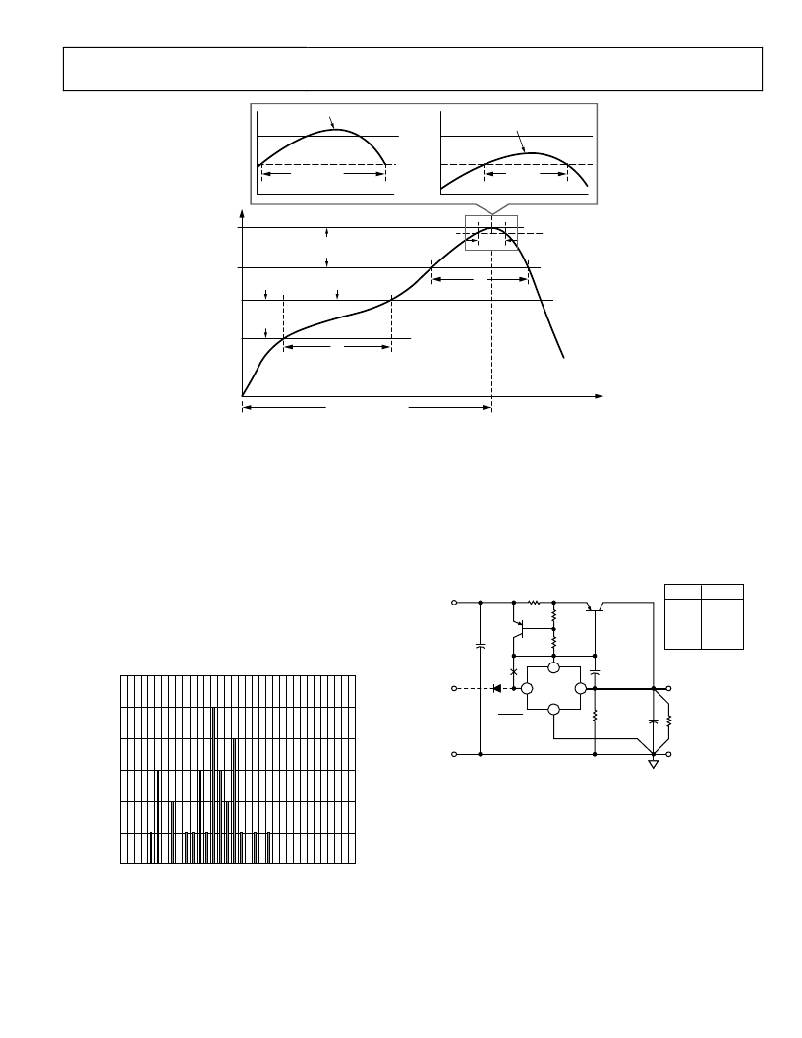
�Figure� 23.� Classification� Profile� (Not� to� Scale)�
�SOLDER� HEAT� EFFECT�
�The� mechanical� stress� and� heat� effect� of� soldering� a� part� to� a�
�PCB� can� cause� output� voltage� of� a� reference� to� shift� in� value.�
�The� output� voltage� of� REF195� shifts� after� the� part� undergoes� the�
�extreme� heat� of� a� lead-free� soldering� profile,� like� the� one� shown�
�in� Figure� 23.� The� materials� that� make� up� a� semiconductor� device�
�and� its� package� have� different� rates� of� expansion� and� contraction.�
�CURRENT-BOOSTED� REFERENCES� WITH� CURRENT�
�LIMITING�
�Whereas� the� 30� mA� rated� output� current� of� the� REF19x� series� is�
�higher� than� is� typical� of� other� reference� ICs,� it� can� be� boosted� to�
�higher� levels,� if� desired,� with� the� addition� of� a� simple� external�
�PNP� transistor,� as� shown� in� Figure� 25.� Full-time� current� limiting� is�
�used� to� protect� the� pass� transistor� against� shorts.�
�The� stress� on� the� dice� has� changed� position,� causing� shift� on� the�
�output� voltage,� after� exposed� to� extreme� soldering� temperatures.�
�This� shift� is� similar� but� more� severe� than� thermal� hysteresis.�
�Typical� result� of� soldering� temperature� effect� on� REF19x� output�
�value� shift� is� shown� in� Figure� 24.� It� shows� the� output� shift� due�
�+V� S� =� 6V�
�TO� 9V�
�(SEE� TEXT)�
�C2�
�100μF�
�Q2�
�2N3906�
�+�
�R4�
�2� ?�
�Q1�
�TIP32A�
�(SEE� TEXT)�
�R1�
�1k� ?�
�R2�
�1.5k� ?�
�OUTPUT� TABLE�
�U1� V� OUT� (V)�
�REF192� 2.5�
�REF193� 3.0�
�REF196� 3.3�
�REF194� 4.5�
�REF195� 5.0�
�F�
�to� soldering� and� does� not� include� mechanical� stress.�
�6�
�5�
�V� C�
�25V�
�D1�
�3�
�1N4148�
�(SEE� TEXT�
�ON� SLEEP)�
�2�
�U1�
�REF196� 6�
�(SEE� TABLE)�
�4�
�R3�
�1.82k� ?�
�C3�
�0.1μF�
�S�
�C1�
�10μF/25V�
�(TANTALUM)�
�+�
�+V� OUT�
�3.3V�
�@� 150mA�
�R1�
�4�
�S�
�3�
�V� S�
�COMMON�
�F�
�V� OUT�
�COMMON�
�Figure� 25.� Boosted� 3.3� V� Referenced� with� Current� Limiting�
�2�
�1�
�0�
�SHIFT� DUE� TO� SOLDER� HEAT� EFFECT� (%)�
�Figure� 24.� Output� Shift� due� to� Solder� Heat� Effect�
�In� this� circuit,� the� power� supply� current� of� reference� U1� flowing�
�through� R1� to� R2� develops� a� base� drive� for� Q1,� whose� collector�
�provides� the� bulk� of� the� output� current.� With� a� typical� gain� of� 100�
�in� Q1� for� 100� mA� to� 200� mA� loads,� U1� is� never� required� to� furnish�
�more� than� a� few� mA,� so� this� factor� minimizes� temperature-related�
�drift.� Short-circuit� protection� is� provided� by� Q2,� which� clamps�
�the� drive� to� Q1� at� about� 300� mA� of� load� current,� with� values� as�
�shown� in� Figure� 25.� With� this� separation� of� control� and� power�
�functions,� dc� stability� is� optimum,� allowing� most� advantageous�
�use� of� premium� grade� REF19x� devices� for� U1.� Of� course,� load�
�Rev.� L� |� Page� 21� of� 28�
�相关PDF资料 |
PDF描述 |
|---|---|
| REF194GSZ-REEL | IC VREF SERIES PREC 4.5V 8-SOIC |
| REF196GSZ-REEL | IC VREF SERIES PREC 3.3V 8-SOIC |
| HBM08DRKF-S13 | CONN EDGECARD 16POS .156 EXTEND |
| GSM11DSEI-S13 | CONN EDGECARD 22POS .156 EXTEND |
| PLX1H470MDL1TD | CAP ALUM 47UF 50V 20% RADIAL |
相关代理商/技术参数 |
参数描述 |
|---|---|
| REF194 | 制造商:AD 制造商全称:Analog Devices 功能描述:Precision Micropower, Low Dropout Voltage References |
| REF1940002SZR | 制造商:Analog Devices 功能描述: |
| REF1940003SR | 制造商:Analog Devices 功能描述: |
| REF1941AIDDCT | 功能描述:Series Voltage Reference IC ±0.1% 20mA SOT-23-5 Thin, TSOT-23-5 制造商:texas instruments 系列:- 包装:剪切带(CT) 零件状态:有效 参考类型:系列 输出类型:固定 电压 - 输出(最小值/固定):4.096V 电压 - 输出(最大值):- 电流 - 输出:20mA 容差:±0.1% 温度系数:25ppm/°C 噪声 - 0.1Hz 至 10Hz:12ppmp-p 噪声 - 10Hz 至 10Hz:- 电压 - 输入:4.116 V ~ 5.5 V 电流 - 电源:460μA 电流 - 阴极:- 工作温度:-55°C ~ 150°C(TJ) 安装类型:表面贴装 封装/外壳:SOT-23-5 细型,TSOT-23-5 供应商器件封装:SOT-5 标准包装:1 |
| REF194ES | 功能描述:IC VREF SERIES PREC 4.5V 8-SOIC RoHS:否 类别:集成电路 (IC) >> PMIC - 电压基准 系列:REF19 标准包装:3,000 系列:- 基准类型:旁路,精度 输出电压:5V 容差:±0.5% 温度系数:100ppm/°C 输入电压:- 通道数:1 电流 - 阴极:80µA 电流 - 静态:- 电流 - 输出:15mA 工作温度:-40°C ~ 85°C 安装类型:表面贴装 封装/外壳:TO-236-3,SC-59,SOT-23-3 供应商设备封装:SOT-23-3 包装:带卷 (TR) 其它名称:LM4040CIM3-5.0MLTRLM4040CIM3-5.0MLTR-ND |
发布紧急采购,3分钟左右您将得到回复。