- 您现在的位置:买卖IC网 > PDF目录16757 > REF194GS-REEL7 (Analog Devices Inc)IC VREF SERIES PREC 4.5V 8-SOIC PDF资料下载
参数资料
| 型号: | REF194GS-REEL7 |
| 厂商: | Analog Devices Inc |
| 文件页数: | 24/28页 |
| 文件大小: | 0K |
| 描述: | IC VREF SERIES PREC 4.5V 8-SOIC |
| 产品变化通告: | Product Discontinuance 27/Oct/2011 |
| 标准包装: | 1,000 |
| 系列: | REF19 |
| 基准类型: | 串联,精度 |
| 输出电压: | 4.5V |
| 容差: | ±10mV |
| 温度系数: | 25ppm/°C |
| 输入电压: | 4.6 V ~ 15 V |
| 通道数: | 1 |
| 电流 - 静态: | 15µA |
| 电流 - 输出: | 30mA |
| 工作温度: | -40°C ~ 85°C |
| 安装类型: | 表面贴装 |
| 封装/外壳: | 8-SOIC(0.154",3.90mm 宽) |
| 供应商设备封装: | 8-SO |
| 包装: | 带卷 (TR) |
第1页第2页第3页第4页第5页第6页第7页第8页第9页第10页第11页第12页第13页第14页第15页第16页第17页第18页第19页第20页第21页第22页第23页当前第24页第25页第26页第27页第28页
�� �
�
�REF19x� Series�
�Data� Sheet�
�Using� dissimilar� REF19x� series� devices� with� this� configuration�
�V� S�
�V� S�
�R� LW�
�A1�
�allows� logic� selection� between� the� U1/U2-specified� terminal�
�voltages.� For� example,� with� U1� (a� REF195)� and� U2� (a� REF196),�
�as� noted� in� the� table� in� Figure� 30,� changing� the� CMOS-compatible�
�V� C� logic� control� voltage� from� high� to� low� selects� between� a� nominal�
�output� of� 5.0� V� and� 3.3� V,� and� vice� versa.� Other� REF19x� family�
�units� can� also� be� used� for� U1/U2,� with� similar� operation� in� a�
�SLEEP�
�3�
�2�
�V� S�
�OUTPUT�
�REF19x�
�GND�
�4�
�6�
�1μF�
�2�
�3�
�R� LW�
�1�
�A1� =� 1/2� OP295�
�100k� ?� 1/2� OP292�
�OP183�
�+V� OUT�
�SENSE�
�+V� OUT�
�FORCE�
�R� L�
�logic� sense,� but� with� outputs� as� per� the� individual� paired� devices�
�(see� the� table� in� Figure� 30).� Of� course,� the� exact� output� voltage�
�tolerance,� drift,� and� overall� quality� of� the� reference� voltage� is�
�consistent� with� the� grade� of� individual� U1� and� U2� devices.�
�Due� to� the� nature� of� the� wire-OR,� one� application� caveat� should�
�be� understood� about� this� circuit.� Because� U1� and� U2� can� only�
�source� current� effectively,� negative� going� output� voltage� changes,�
�which� require� the� sinking� of� current,� necessarily� take� longer� than�
�positive� going� changes.� In� practice,� this� means� that� the� circuit� is�
�quite� fast� when� undergoing� a� transition� from� 3.3� V� to� 5� V,� but� the�
�transition� from� 5� V� to� 3.3� V� takes� longer.� Exactly� how� much�
�longer� is� a� function� of� the� load� resistance,� R� L� ,� seen� at� the� output� and�
�the� typical� 1� μF� value� of� C2.� In� general,� a� conservative� transition�
�time� is� approximately� several� milliseconds� for� load� resistances�
�in� the� range� of� 100� Ω� to� 1� kΩ.� Note� that� for� highest� accuracy� at�
�the� new� output� voltage,� several� time� constants� should� be� allowed�
�(for� example,� >7.6� time� constants� for� <1/2� LSB� error� @� 10� bits).�
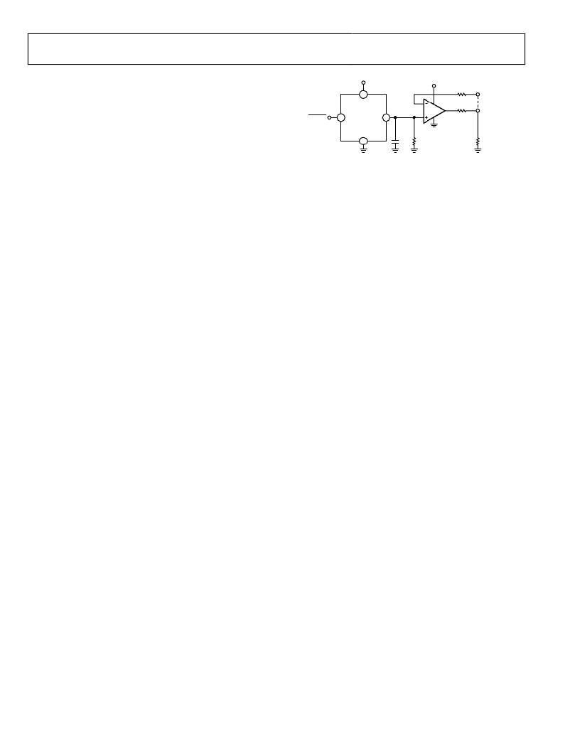
�KELVIN� CONNECTIONS�
�In� many� portable� applications� where� the� PCB� cost� and� area� go�
�hand-in-hand,� circuit� interconnects� are� very� often� narrow.� These�
�narrow� lines� can� cause� large� voltage� drops� if� the� voltage� reference� is�
�required� to� provide� load� currents� to� various� functions.� The� inter-�
�connections� of� a� circuit� can� exhibit� a� typical� line� resistance� of�
�0.45� mΩ/square� (for� example,� 1� oz.� Cu).�
�In� applications� where� these� devices� are� configured� as� low� dropout�
�voltage� regulators,� these� wiring� voltage� drops� can� become� a� large�
�source� of� error.� To� circumvent� this� problem,� force� and� sense�
�connections� can� be� made� to� the� reference� through� the� use� of� an�
�operational� amplifier,� as� shown� in� Figure� 31.� This� method� provides�
�a� means� by� which� the� effects� of� wiring� resistance� voltage� drops� can�
�be� eliminated.� Load� currents� flowing� through� wiring� resistance�
�produce� an� I-R� error� (I� LOAD� � R� WIRE� )� at� the� load.� However,� the�
�Kelvin� connection� overcomes� the� problem� by� including� the�
�wiring� resistance� within� the� forcing� loop� of� the� op� amp.� Because�
�the� op� amp� senses� the� load� voltage,� op� amp� loop� control� forces�
�the� output� to� compensate� for� the� wiring� error� and� to� produce�
�the� correct� voltage� at� the� load.� Depending� on� the� reference�
�device� chosen,� operational� amplifiers� that� can� be� used� in� this�
�Figure� 31.� Low� Dropout,� Kelvin-Connected� Voltage� Reference�
�FAIL-SAFE� 5� V� REFERENCE�
�Some� critical� applications� require� a� reference� voltage� to� be�
�maintained� at� a� constant� voltage,� even� with� a� loss� of� primary�
�power.� The� low� standby� power� of� the� REF19x� series� and� the�
�switched� output� capability� allow� a� fail-safe� reference� con-�
�figuration� to� be� implemented� rather� easily.� This� reference�
�maintains� a� tight� output� voltage� tolerance� for� either� a� primary�
�power� source� (ac� line� derived)� or� a� standby� (battery� derived)�
�power� source,� automatically� switching� between� the� two� as� the�
�power� conditions� change.�
�The� circuit� in� Figure� 32� illustrates� this� concept,� which� borrows�
�from� the� switched� output� idea� of� Figure� 30,� again� using� the�
�REF19x� device� family� output� wire-OR� capability.� In� this� case,�
�because� a� constant� 5� V� reference� voltage� is� desired� for� all� condi-�
�tions,� two� REF195� devices� are� used� for� U1� and� U2,� with� their�
�on/off� switching� controlled� by� the� presence� or� absence� of� the�
�primary� dc� supply� source,� V� S� .� V� BAT� is� a� 6� V� battery� backup�
�source� that� supplies� power� to� the� load� only� when� V� S� fails.� For�
�normal� (V� S� present)� power� conditions,� V� BAT� sees� only� the� 15� μA�
�(maximum)� standby� current� drain� of� U1� in� its� off� state.�
�In� operation,� it� is� assumed� that� for� all� conditions,� either� U1� or�
�U2� is� on,� and� a� 5� V� reference� output� is� available.� With� this�
�voltage� constant,� a� scaled� down� version� is� applied� to� the�
�Comparator� IC� U3,� providing� a� fixed� 0.5� V� input� to� the� negative�
�input� for� all� power� conditions.� The� R1� to� R2� divider� provides� a�
�signal� to� the� U3� positive� input� proportionally� to� V� S� ,� which�
�switches� U3� and� U1/U2,� dependent� upon� the� absolute� level� of�
�V� S� .� In� Figure� 32,� Op� Amp� U3� is� configured� as� a� comparator�
�with� hysteresis,� which� provides� clean,� noise-free� output�
�switching.� This� hysteresis� is� important� to� eliminate� rapid�
�switching� at� the� threshold� due� to� V� S� ripple.� Furthermore,� the�
�device� chosen� is� the� AD820,� a� rail-to-rail� output� device.� This�
�device� provides� high� and� low� output� states� within� a� few� mV� of�
�V� S� ,� ground� for� accurate� thresholds,� and� compatible� drive� for� U2�
�for� all� V� S� conditions.� R3� provides� positive� feedback� for� circuit�
�hysteresis,� changing� the� threshold� at� the� positive� input� as� a�
�function� of� the� output� of� U3.�
�application� are� the� OP295,� OP292,� and� OP183.�
�Rev.� L� |� Page� 24� of� 28�
�相关PDF资料 |
PDF描述 |
|---|---|
| V4-3.5-0-SP-SM | HEAT SHRINK TUBING |
| RBM15DRMI | CONN EDGECARD 30POS .156 SQ WW |
| 322A158-4/86-0 | BOOT MOLDED |
| RBC26DRES | CONN EDGECARD 52POS .100 EYELET |
| V4-4.0-0-SP-SM | HEAT SHRINK TUBING BLACK 1000M |
相关代理商/技术参数 |
参数描述 |
|---|---|
| REF194GSZ | 功能描述:IC VREF SERIES PREC 4.5V 8-SOIC RoHS:是 类别:集成电路 (IC) >> PMIC - 电压基准 系列:REF19 标准包装:3,000 系列:- 基准类型:旁路,精度 输出电压:3V 容差:±0.5% 温度系数:100ppm/°C 输入电压:- 通道数:1 电流 - 阴极:82µA 电流 - 静态:- 电流 - 输出:15mA 工作温度:-40°C ~ 85°C 安装类型:表面贴装 封装/外壳:6-TSSOP(5 引线),SC-88A,SOT-353 供应商设备封装:SC-70-5 包装:带卷 (TR) 其它名称:296-20888-2 |
| REF194GSZ-REEL | 功能描述:IC VREF SERIES PREC 4.5V 8-SOIC RoHS:是 类别:集成电路 (IC) >> PMIC - 电压基准 系列:REF19 产品培训模块:Voltage Reference Basics 标准包装:100 系列:- 基准类型:旁路,精度 输出电压:4.096V 容差:±0.075% 温度系数:50ppm/°C 输入电压:- 通道数:1 电流 - 阴极:1µA 电流 - 静态:- 电流 - 输出:10mA 工作温度:0°C ~ 70°C 安装类型:表面贴装 封装/外壳:8-SOIC(0.154",3.90mm 宽) 供应商设备封装:8-SOIC 包装:管件 |
| REF194GSZ-REEL7 | 功能描述:IC VREF SERIES PREC 4.5V 8SOIC RoHS:是 类别:集成电路 (IC) >> PMIC - 电压基准 系列:REF19 标准包装:3,000 系列:- 基准类型:旁路,精度 输出电压:3V 容差:±0.5% 温度系数:100ppm/°C 输入电压:- 通道数:1 电流 - 阴极:82µA 电流 - 静态:- 电流 - 输出:15mA 工作温度:-40°C ~ 85°C 安装类型:表面贴装 封装/外壳:6-TSSOP(5 引线),SC-88A,SOT-353 供应商设备封装:SC-70-5 包装:带卷 (TR) 其它名称:296-20888-2 |
| REF195 | 制造商:AD 制造商全称:Analog Devices 功能描述:Precision Micropower, Low Dropout, Voltage References |
| REF1950008S | 制造商:Analog Devices 功能描述: |
发布紧急采购,3分钟左右您将得到回复。