- 您现在的位置:买卖IC网 > PDF目录20734 > REF194GSZ (Analog Devices Inc)IC VREF SERIES PREC 4.5V 8-SOIC PDF资料下载
参数资料
| 型号: | REF194GSZ |
| 厂商: | Analog Devices Inc |
| 文件页数: | 23/28页 |
| 文件大小: | 0K |
| 描述: | IC VREF SERIES PREC 4.5V 8-SOIC |
| 标准包装: | 98 |
| 系列: | REF19 |
| 基准类型: | 串联,精度 |
| 输出电压: | 4.5V |
| 容差: | ±10mV |
| 温度系数: | 25ppm/°C |
| 输入电压: | 4.6 V ~ 15 V |
| 通道数: | 1 |
| 电流 - 静态: | 15µA |
| 电流 - 输出: | 30mA |
| 工作温度: | -40°C ~ 85°C |
| 安装类型: | 表面贴装 |
| 封装/外壳: | 8-SOIC(0.154",3.90mm 宽) |
| 供应商设备封装: | 8-SO |
| 包装: | 管件 |
| 产品目录页面: | 797 (CN2011-ZH PDF) |
第1页第2页第3页第4页第5页第6页第7页第8页第9页第10页第11页第12页第13页第14页第15页第16页第17页第18页第19页第20页第21页第22页当前第23页第24页第25页第26页第27页第28页
�� �
�
�Data� Sheet�
�Although� this� concept� is� simple,� some� cautions� are� needed.� Because�
�the� lower� reference� circuit� must� sink� a� small� bias� current� from� U2�
�(50� μA� to� 100� μA),� plus� the� base� current� from� the� series� PNP� output�
�transistor� in� U2,� either� the� external� load� of� U1� or� R1� must� provide�
�a� path� for� this� current.� If� the� U1� minimum� load� is� not� well� defined,�
�V� S�
�2�
�V� S�
�REF19x�
�REF19x� Series�
�Resistor� R1� should� be� used,� set� to� a� value� that� conservatively� passes�
�3�
�SLEEP�
�OUTPUT� 6�
�R1�
�GND�
�I� SY�
�ADJUST�
�V� IN� ≥� I� OUT� ×� R� L� (MAX)� +� V� SY� (MIN)�
�I� OUT� =� +� I� SY� (REF19x)�
�>>� I� SY�
�R� SET�
�600� μA� of� current� with� the� applicable� V� OUT1� across� it.� Note� that� the�
�two� U1� and� U2� reference� circuits� are� locally� treated� as� macrocells,�
�each� having� its� own� bypasses� at� input� and� output� for� best� stability.�
�Both� U1� and� U2� in� this� circuit� can� source� dc� currents� up� to�
�their� full� rating.� The� minimum� input� voltage,� V� S� ,� is� determined� by�
�the� sum� of� the� outputs,� V� OUT2� ,� plus� the� dropout� voltage� of� U2.�
�A� related� variation� on� stacking� two� 3-terminal� references� is� shown�
�in� Figure� 28,� where� U1,� a� REF192,� is� stacked� with� a� 2-terminal�
�reference� diode,� such� as� the� AD589.� Like� the� 3-terminal� stacked�
�reference� shown� in� Figure� 27,� this� circuit� provides� two� outputs,�
�V� OUT1� and� V� OUT2� ,� which� are� the� individual� terminal� voltages� of� D1�
�and� U1,� respectively.� Here� this� is� 1.235� V� and� 2.5� V,� which� provides� a�
�V� OUT2� of� 3.735� V.� When� using� 2-terminal� reference� diodes,� such� as�
�D1,� the� rated� minimum� and� maximum� device� currents� must� be�
�observed,� and� the� maximum� load� current� from� V� OUT1� can� be� no�
�greater� than� the� current� setup� by� R1� and� V� O� (U1).� When� V� O�
�(U1)� is� equal� to� 2.5� V,� R1� provides� a� 500� μA� bias� to� D1,� so� the�
�maximum� load� current� available� at� V� OUT1� is� 450� μA� or� less.�
�+V� S�
�V� S� >� V� OUT2� +� 0.15V�
�2�
�1μF�
�4� R� SET�
�P1�
�I� OUT�
�V� OUT� R� L�
�R� SET�
�V� OUT� FOR� EXAMPLE,� REF195:� V� OUT� =� 5V�
�I� OUT� =� 5mA�
�R1� =� 953� ?�
�P1� =� 100� ?� ,� 10-TURN�
�Figure� 29.� A� Low� Dropout,� Precision� Current� Source�
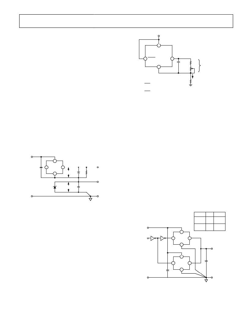
�SWITCHED� OUTPUT� 5� V/3.3� V� REFERENCE�
�Applications� often� require� digital� control� of� reference� voltages,�
�selecting� between� one� stable� voltage� and� a� second.� With� the�
�sleep� feature� inherent� to� the� REF19x� series,� switched� output�
�reference� configurations� are� easily� implemented� with� little�
�additional� hardware.�
�The� circuit� in� Figure� 30� shows� the� general� technique,� which� takes�
�advantage� of� the� output� wire-OR� capability� of� the� REF19x� device�
�family.� When� off,� a� REF19x� device� is� effectively� an� open� circuit�
�at� the� output� node� with� respect� to� the� power� supply.� When� on,� a�
�REF19x� device� can� source� current� up� to� its� current� rating,� but�
�C1�
�0.1� μ� F�
�3�
�U1�
�REF192�
�4�
�6�
�V� O� (U1)�
�+�
�C2�
�1� μ� F�
�R1�
�4.99k� Ω�
�(SEE� TEXT)�
�+V� OUT2�
�3.735V�
�sink� only� a� few� μA� (essentially,� just� the� relatively� low� current� of� the�
�internal� output� scaling� divider).� Consequently,� when� two� devices�
�are� wired� together� at� their� common� outputs,� the� output� voltage�
�+� C3�
�D1�
�V� O� (D1)�
�+V� OUT1�
�1.235V�
�AD589� 1� μ� F�
�V� IN�
�COMMON�
�V� OUT�
�COMMON�
�Figure� 28.� Stacking� Voltage� References� with� the� REF192�
�PRECISION� CURRENT� SOURCE�
�is� the� same� as� the� output� voltage� for� the� on� device.� The� off� state�
�device� draws� a� small� standby� current� of� 15� μA� (maximum),� but�
�otherwise� does� not� interfere� with� operation� of� the� on� device,� which�
�can� operate� to� its� full� current� rating.� Note� that� the� two� devices� in�
�the� circuit� conveniently� share� both� input� and� output� capacitors,�
�and� with� CMOS� logic� drive,� it� is� power� efficient.�
�OUTPUT� TABLE�
�In� low� power� applications,� the� need� often� arises� for� a� precision�
�U1/U2�
�V� C� *�
�V� OUT� (V)�
�current� source� that� can� operate� on� low� supply� voltages.� As�
�shown� in� Figure� 29,� any� one� of� the� devices� in� the� REF19x� family�
�of� references� can� be� configured� as� a� precision� current� source.�
�The� circuit� configuration� illustrated� is� a� floating� current� source�
�with� a� grounded� load.� The� output� voltage� of� the� reference� is�
�bootstrapped� across� R� SET� ,� which� sets� the� output� current� into� the�
�+V� S� =� 6V�
�V� C�
�1� 2� 3� 4�
�U3A� U3B�
�74HC04� 74HC04�
�3�
�2�
�U1�
�REF19x�
�(SEE� TABLE)�
�4�
�6�
�REF195/� HIGH� 5.0�
�REF196� LOW� 3.3�
�REF194/� HIGH� 4.5�
�REF195� LOW� 5.0�
�*CMOS� LOGIC� LEVELS�
�load.� With� this� configuration,� circuit� precision� is� maintained� for�
�load� currents� in� the� range� from� the� reference’s� supply� current�
�+V� OUT�
�(typically� 30� μA)� to� approximately� 30� mA.� The� low� dropout�
�voltage� of� these� devices� maximizes� the� current� source’s� output�
�voltage� compliance� without� excess� headroom.�
�C1�
�0.1μF�
�3�
�2�
�U2�
�REF19x�
�(SEE� TABLE)�
�4�
�6�
�+� C2�
�1μF�
�V� IN�
�COMMON�
�Rev.� L� |� Page� 23� of� 28�
�Figure� 30.� Switched� Output� Reference�
�V� OUT�
�COMMON�
�相关PDF资料 |
PDF描述 |
|---|---|
| TPSV477M006R0055 | CAP TANT 470UF 6.3V 20% 2924 |
| RW2-4812S/SMD | CONV DC/DC 2W 36-72VIN 12VOUT |
| HBC05DRTS | CONN EDGECARD 10POS DIP .100 SLD |
| FMC19DRXN | CONN EDGECARD 38POS DIP .100 SLD |
| REF196GSZ | IC VREF SERIES PREC 3.3V 8-SOIC |
相关代理商/技术参数 |
参数描述 |
|---|---|
| REF194GSZ-REEL | 功能描述:IC VREF SERIES PREC 4.5V 8-SOIC RoHS:是 类别:集成电路 (IC) >> PMIC - 电压基准 系列:REF19 产品培训模块:Voltage Reference Basics 标准包装:100 系列:- 基准类型:旁路,精度 输出电压:4.096V 容差:±0.075% 温度系数:50ppm/°C 输入电压:- 通道数:1 电流 - 阴极:1µA 电流 - 静态:- 电流 - 输出:10mA 工作温度:0°C ~ 70°C 安装类型:表面贴装 封装/外壳:8-SOIC(0.154",3.90mm 宽) 供应商设备封装:8-SOIC 包装:管件 |
| REF194GSZ-REEL7 | 功能描述:IC VREF SERIES PREC 4.5V 8SOIC RoHS:是 类别:集成电路 (IC) >> PMIC - 电压基准 系列:REF19 标准包装:3,000 系列:- 基准类型:旁路,精度 输出电压:3V 容差:±0.5% 温度系数:100ppm/°C 输入电压:- 通道数:1 电流 - 阴极:82µA 电流 - 静态:- 电流 - 输出:15mA 工作温度:-40°C ~ 85°C 安装类型:表面贴装 封装/外壳:6-TSSOP(5 引线),SC-88A,SOT-353 供应商设备封装:SC-70-5 包装:带卷 (TR) 其它名称:296-20888-2 |
| REF195 | 制造商:AD 制造商全称:Analog Devices 功能描述:Precision Micropower, Low Dropout, Voltage References |
| REF1950008S | 制造商:Analog Devices 功能描述: |
| REF1950009S | 制造商:Analog Devices 功能描述: |
发布紧急采购,3分钟左右您将得到回复。