- 您现在的位置:买卖IC网 > PDF目录385770 > RF3322PCBA (RF Micro Devices, Inc.) CABLE REVERSE PATH PROGRAMMABLE GAIN AMPLIFIER PDF资料下载
参数资料
| 型号: | RF3322PCBA |
| 厂商: | RF Micro Devices, Inc. |
| 英文描述: | CABLE REVERSE PATH PROGRAMMABLE GAIN AMPLIFIER |
| 中文描述: | 电缆反向路径可编程增益放大器 |
| 文件页数: | 7/14页 |
| 文件大小: | 169K |
| 代理商: | RF3322PCBA |
Preliminary
3-33
RF3322
Rev A2 010518
3
L
A
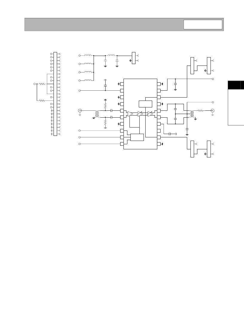
Evaluation Board S chematic
PCB Layout Considerations
The RF3322 evaluation board can be used as a guide for the layout in your application. Care should be taken in laying
out the RF3322 in other applications. The RF3322 will have similar results if the following guidelines are taken into con-
sideration:
Make sure underside of package is soldered to a good ground on the PCB.
Move C2, C9, C10, and C11 as close to T1 as possible.
Keep input and output traces as short as possible.
Ensure a good ground plane by using multiple vias to the ground plane.
Use a low noise power supply along with decoupling capacitors.
16
15
18
17
20
19
14
13
12
11
5
6
3
4
1
2
7
8
9
10
C3
1 nF
C4
1 nF
C7
220 pF
T2
4:1
C9
100 pF
Gain Control
and Serial Bus
Power
Control
C11
15 pF
C10
15 pF
R6
24
J7
RF OUT
VCC3
VCC2
C6
0.1
μ
F
T1
1:1
R5
75
R4
75
J2
RF IN
VCC1
C5
0.1
μ
F
CS
SDA
SCLK
1
2
3
4
5
6
7
8
9
10
11
12
13
14
15
16
17
18
19
20
21
22
23
24
25
R1
100 k
R2
100 k
VCC
NC
CS
SDA
SCLK
SHDN
TXEN
NC
NC
NC
NC
NC
GND
GND
GND
GND
GND
GND
GND
GND
VCC
NC
NC
VCC
NC
CS
SDA
SCLK
J5-1
J3-1
J1
J3
1
2
3
J1-6
TXEN
J4
1
2
3
VCC
GND
J5
1
2
3
J1-5
SHDN
J6
1
2
3
VCC
GND
JP1
1
2
VCC
GND
+
C2
1 nF
L1 (Ferrite)
30
C1
10
μ
F
(10 V)
L3 (Ferrite)
30
L4 (Ferrite)
30
L5 (Ferrite)
30
L2 (Ferrite)
30
VCC
VCC1
VCC2
VCC3
Notes:
1. 4-layer board. 2nd layer is ground plane.
2. Place C5 and C6 as close to pin as possible.
3. C1 is tantalum, size code Y.
4. All other components are 0603 size.
5. Replace R6 with 0
resistor if 75
connector is used.
3322410-
相关PDF资料 |
PDF描述 |
|---|---|
| RF3330 | IF GAIN CONTROLLED AMPLIFIER |
| RF3330PCBA | IF GAIN CONTROLLED AMPLIFIER |
| RF3374 | GENERAL PURPOSE AMPLIFIER |
| RF3374PCBA-410 | GENERAL PURPOSE AMPLIFIER |
| RF3404 | DUAL-BAND/TRI-MODE CDMA LOW NOISE AMPLIFIER/MIXER MODULE |
相关代理商/技术参数 |
参数描述 |
|---|---|
| RF3323-000 | 制造商:TE Connectivity 功能描述:- Bag |
| RF3324-000 | 制造商:TE Connectivity 功能描述:FUSE 100A 16V 2PIN - Bag |
| RF3326-000 | 制造商:TE Connectivity 功能描述:- Bag |
| RF3327-000 | 制造商:TE Connectivity 功能描述:- Tape and Reel |
| RF3328-000 | 制造商:TE Connectivity 功能描述:AHRF050 - Bag |
发布紧急采购,3分钟左右您将得到回复。