- 您现在的位置:买卖IC网 > PDF目录18777 > RFRXD0420-I/LQ (Microchip Technology)MODULE RCVR 315/433MHZ ASK/FSK PDF资料下载
参数资料
| 型号: | RFRXD0420-I/LQ |
| 厂商: | Microchip Technology |
| 文件页数: | 6/32页 |
| 文件大小: | 0K |
| 描述: | MODULE RCVR 315/433MHZ ASK/FSK |
| 产品变化通告: | RFRXD0(4,9)20I/LQ Obsolescence 07/Mar/2012 |
| 标准包装: | 250 |
| 频率: | 300MHz ~ 450MHz |
| 灵敏度: | -106dBm |
| 数据传输率 - 最大: | 80 kbps |
| 调制或协议: | ASK,FM,FSK |
| 应用: | 家庭自动化,遥感,RKE |
| 电流 - 接收: | 9.2mA |
| 数据接口: | PCB,表面贴装 |
| 天线连接器: | PCB,表面贴装 |
| 电源电压: | 2.5 V ~ 5.5 V |
| 工作温度: | -40°C ~ 85°C |
| 封装/外壳: | 32-LQFP |
| 供应商设备封装: | 32-LQFP(7x7) |
| 包装: | 托盘 |
| 产品目录页面: | 685 (CN2011-ZH PDF) |
| 配用: | DV164102-ND - KIT DEV RFPICKIT KIT 1 |
| 其它名称: | RFRXD0420-I/LQR RFRXD0420-I/LQR-ND |
第1页第2页第3页第4页第5页当前第6页第7页第8页第9页第10页第11页第12页第13页第14页第15页第16页第17页第18页第19页第20页第21页第22页第23页第24页第25页第26页第27页第28页第29页第30页第31页第32页
�� �
�
�rfRXD0420/0920�
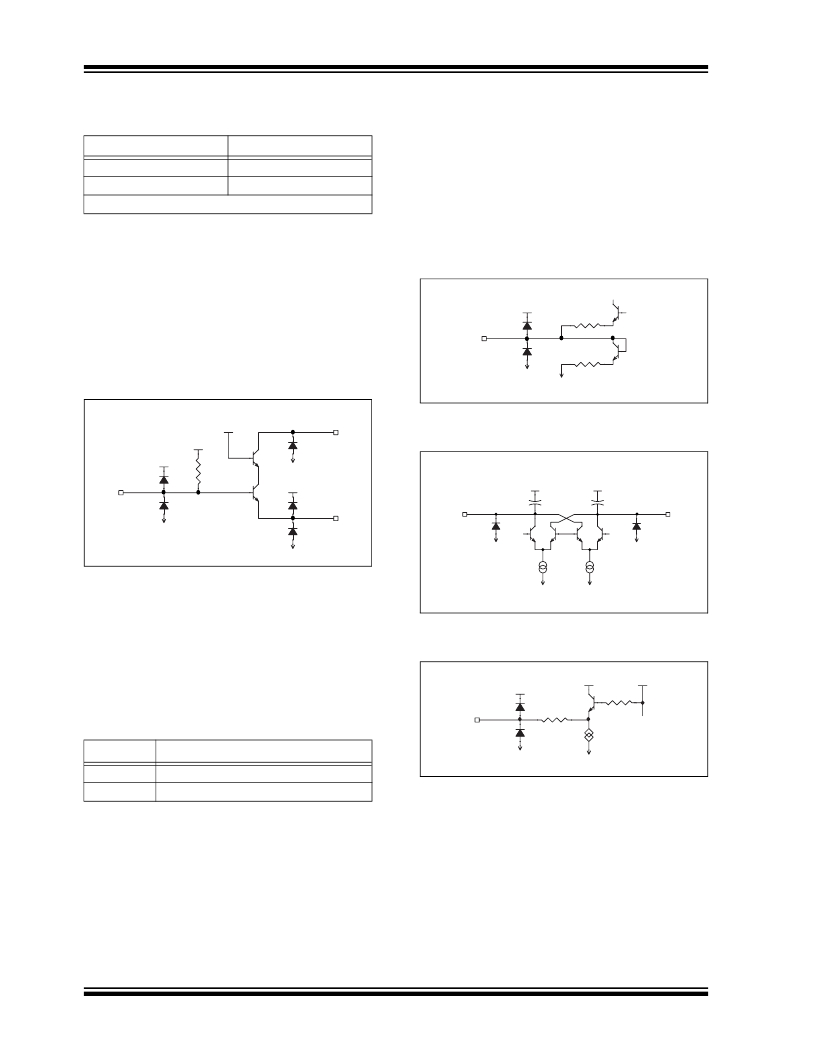
�Approximate� LNA� noise� figures� are� listed� in� Table� 2-3.�
�The� 1IF+� (Pin� 6)� and� 1IF-� (Pin� 7)� are� bias� connections�
�TABLE� 2-3:�
�LNA� NOISE� FIGURES�
�to� the� MIXER1� balanced� collectors.� Both� pins� are�
�open-collector� outputs� and� are� individually� pulled� up� to�
�Device�
�rfRXD0420�
�rfRXD0920�
�Note� 1:� Approximate� value�
�Noise� Figure� (1)�
�TBD�
�TBD�
�V� DD� by� a� load� resistor.� The� MIXER1� bias� pins� are� illus-�
�trated� in� Figure� 2-5.�
�1IF� OUT� (Pin� 9)� has� an� approximately� 330� ?� single-�
�ended� output� impedance.� The� 330� ?� impedance�
�provides� a� direct� match� to� low� cost� ceramic� IF� filters.�
�The� 1IF� OUT� pins� is� illustrated� in� Figure� 2-6.�
�LNA� IN� (Pin� 31)� has� an� input� impedance� of� approxi-�
�mately� 26� ?� ||� 2� pF� single-ended.�
�LNA� OUT� (Pin� 3)� has� an� open-collector� output� and� is�
�pulled� up� to� V� DD� via� a� tuned� circuit.�
�FIGURE� 2-4:�
�BLOCK� DIAGRAM� OF� MIXER1�
�PIN�
�Important:� To� ensure� LNA� stability� the� V� SS� pin� (Pin� 1)�
�must� be� connected� to� a� low� impedance� ground.�
�The� LNA� pins� are� illustrated� in� Figure� 2-3.�
�1IF� IN�
�4�
�V� DD�
�13� ?�
�13� ?�
�FIGURE� 2-3:�
�BLOCK� DIAGRAM� OF� LNA�
�PINS�
�V� SS�
�V� SS�
�500� μ� A�
�V� DD�
�1.6V�
�0.8V�
�5� k� ?�
�V� SS�
�LNA� OUT�
�3�
�FIGURE� 2-5:�
�BLOCK� DIAGRAM� OF� MIXER1�
�BIAS� PINS�
�LNA� IN�
�V� DD�
�V� DD�
�V� DD�
�31�
�V� SS�
�V� SS�
�1�
�1IF+�
�6�
�20� pF�
�20� pF�
�1IF-�
�7�
�V� SS�
�The� gain� of� the� LNA� can� be� selected� between� High� and�
�Low� Gain� modes� by� the� LNA� GAIN� pin� (Pin� 2).� LNA� GAIN�
�is� a� CMOS� input� with� hysteresis.� Table� 2-4� summarizes�
�V� SS�
�500� μ� A�
�V� SS�
�500� μ� A�
�V� SS�
�V� SS�
�the� voltage� levels� and� modes� for� LNA� gain.�
�In� the� High� Gain� mode� the� LNA� operates� normally.� In�
�Low� Gain� mode� the� gain� of� the� LNA� is� reduced� approx-�
�FIGURE� 2-6:�
�BLOCK� DIAGRAM� OF� IF�
�PREAMP� PIN�
�imately� 25� dB,� reduces� total� supply� current,� and�
�increases� maximum� input� signal� levels� (see� Electrical�
�V� DD�
�V� DD�
�6.8� k� ?�
�V� DD�
�Characteristics� section� for� values).�
�TABLE� 2-4:� LNA� GAIN� CONTROL�
�1IF� OUT�
�9�
�130� ?�
�230� μ� A�
�LNA� GAIN�
�<� 0.8� V�
�Description�
�High� Gain� mode�
�V� SS�
�V� SS�
�>� 1.4� V�
�Low� Gain� mode�
�2.5�
�IF� Limiting� Amplifier� with� RSSI�
�2.4�
�MIXER1� and� IF� Preamp�
�The� IF� Limiting� Amplifier� amplifies� and� limits� the� IF�
�signal� at� the� 2IF� IN� pin� (Pin� 11).� It� also� generates� the�
�MIXER1� performs� down-conversion� of� the� RF� signal� to�
�the� Intermediate� Frequency� (IF)� and� is� followed� by� an�
�Received� Signal� Strength� Indicator� (RSSI)� signal�
�(Pin� 21).�
�IF� preamplifier.�
�1IF� IN� (Pin� 4)� has� an� approximately� 33� ?� single-ended�
�2.5.1�
�IF� LIMITING� AMPLIFIER�
�input� impedance.� The� 1IF� IN� pin� is� illustrated� in� Figure� 2-�
�4.�
�Magnitude� control� circuitry� is� used� in� the� last� stage� of�
�the� receiver� to� keep� the� signal� constant� for� demodula-�
�tion.� It� can� consist� of� a� limiting� or� Automatic� Gain�
�Control� (AGC)� amplifier.� A� limiting� amplifier� is�
�DS70090A-page� 6�
�Preliminary�
�?� 2003� Microchip� Technology� Inc.�
�相关PDF资料 |
PDF描述 |
|---|---|
| M50100TB1600 | MODULE POWER 100A 1600V 3PH BRDG |
| RXM-900-HP3-SPS | RECEIVER RF 902-928MHZ 8P/100S |
| M50100SB1600 | MODULE POWER 100A 1600V BRIDGE |
| M50100TB400 | MODULE POWER 100A 400V 3PH BRDG |
| M5060TB1600 | MODULE POWER 60A 1600V 3PH BRDG |
相关代理商/技术参数 |
参数描述 |
|---|---|
| RFRXD0420T-I/LQ | 功能描述:射频收发器 33 LD 300-450 MHz RF RoHS:否 制造商:Atmel 频率范围:2322 MHz to 2527 MHz 最大数据速率:2000 Kbps 调制格式:OQPSK 输出功率:4 dBm 类型: 工作电源电压:1.8 V to 3.6 V 最大工作温度:+ 85 C 接口类型:SPI 封装 / 箱体:QFN-32 封装:Tray |
| RFRXD0920 | 制造商:MICROCHIP 制造商全称:Microchip Technology 功能描述:UHF ASK/FSK/FM Receiver |
| RFRXD0920-I/LQ | 功能描述:射频接收器 868/915 MHz ASK/FSKB RoHS:否 制造商:Skyworks Solutions, Inc. 类型:GPS Receiver 封装 / 箱体:QFN-24 工作频率:4.092 MHz 工作电源电压:3.3 V 封装:Reel |
| RFRXD0920T-I/LQ | 功能描述:射频收发器 32 LD 800-930 MHz RF RoHS:否 制造商:Atmel 频率范围:2322 MHz to 2527 MHz 最大数据速率:2000 Kbps 调制格式:OQPSK 输出功率:4 dBm 类型: 工作电源电压:1.8 V to 3.6 V 最大工作温度:+ 85 C 接口类型:SPI 封装 / 箱体:QFN-32 封装:Tray |
| RFS04ZG-M6 | 制造商:Power-One 功能描述: |
发布紧急采购,3分钟左右您将得到回复。