- 您现在的位置:买卖IC网 > PDF目录299869 > RH137MH (LINEAR TECHNOLOGY CORP) 1.2 V-22 V ADJUSTABLE NEGATIVE REGULATOR, MBCY3 PDF资料下载
参数资料
| 型号: | RH137MH |
| 厂商: | LINEAR TECHNOLOGY CORP |
| 元件分类: | 可调负电压单路输出标准稳压器 |
| 英文描述: | 1.2 V-22 V ADJUSTABLE NEGATIVE REGULATOR, MBCY3 |
| 封装: | METAL CAN, TO-39, 3 PIN |
| 文件页数: | 3/4页 |
| 文件大小: | 63K |
| 代理商: | RH137MH |
RH137
3
Information furnished by Linear Technology Corporation is believed to be accurate and reliable.
However, no responsibility is assumed for its use. Linear Technology Corporation makes no represen-
tation that the interconnection of its circuits as described herein will not infringe on existing patent rights.
TABLE 1A: ELECTRICAL CHARACTERISTICS (Postirradiation) (Note 4)
Note 1: Unless otherwise specified, these specifications apply for
VIN – VOUT= 5V; and IOUT = 0.1A for the H package (TO-39) and
IOUT = 0.5A for the K package (TO-3) package. Although power dissipation
is internally limited, these specifications are applicable for power
dissipations of 2W for the TO-39 and 20W for the TO-3. IMAX is 0.2A for
the TO-39 and 1.5A for the TO-3 package.
Note 2: Regulation is measured at a constant junction temperature using
pulse testing with a low duty cycle. Changes in output voltage due to
heating effects are covered under the specification for thermal regulation.
Note 3: Guaranteed by design, characterization or correlation to other
tested parameters.
Note 4: TJ = 25°C unless otherwise noted.
Note 5: ISC is tested at the ambient temperatures of 25°C and –55°C. ISC
cannot be tested at the maximum ambient temperature of 150
°C due to
the high power level required. ISC specification at 150°C ambient is
guaranteed by characterization and correlation to 25
°C testing.
MIL-STD-883 TEST REQUIREMENTS
SUBGROUP
Final Electrical Test Requirements (Method 5004)
1*,2,3
Group A Test Requirements (Method 5005)
1,2,3
Group B and D End Point Electrical Parameters
1,2,3
(Method 5005)
* PDA Applies to subgroup 1. See PDA Test Notes.
PDA Test Notes
The PDA is specified as 5% based on failures from group A, subgroup 1,
tests after cooldown as the final electrical test in accordance with method
5004 of MIL-STD-883. The verified failures of group A, subgroup 1, after
burn-in divided by the total number of devices submitted for burn-in in
that lot shall be used to determine the percent for the lot.
Linear Technology Corporation reserves the right to test to tighter limits
than those given.
TABLE 2: ELECTRICAL TEST REQUIRE E TS
UW
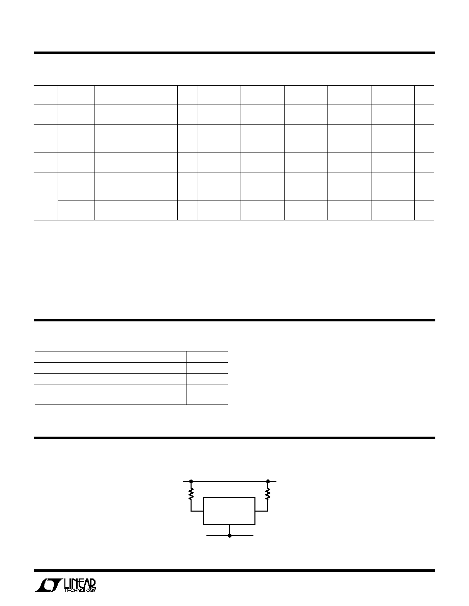
TOTAL DOSE BIAS CIRCUIT
RH137
+15V
VIN
243
Ω
2k
2
1
ADJ
–15V
RH137 TDBC
OUTPUT
CASE
10KRAD(Si)
20KRAD(Si)
50KRAD(Si)
100KRAD(Si)
200KRAD(Si)
SYMBOL PARAMETER CONDITIONS
NOTES MIN
MAX
MIN
MAX
MIN
MAX
MIN
MAX
MIN
MAX
UNITS
IADJ
Adjust Pin
100
μA
Current
ΔIADJ
Adjust Pin
10mA
≤ IOUT ≤ IMAX
55
5
μA
Current
3V
≤ VIN – VOUT ≤ 30V
55
5
μA
Change
IMIN
Minimum
VIN – VOUT = 30V
5
mA
Load Current
VIN – VOUT ≤ 10V
33
3
mA
Current Limit
H Package
VIN – VOUT ≤ 15V
0.5
A
VIN – VOUT = 30V
0.15
A
K Package
VIN – VOUT ≤ 15V
1.5
A
VIN – VOUT = 30V
0.24
A
相关PDF资料 |
PDF描述 |
|---|---|
| RH137MK | 1.2 V-22 V ADJUSTABLE NEGATIVE REGULATOR, MBFM2 |
| RH200-P | Coreless Coil Current Transducer RH 100~1000-P |
| RH200-S | Coreless Coil Current Transducer RH 100~1000-S |
| RH500-S | Coreless Coil Current Transducer RH 100~1000-S |
| RH500-P | Coreless Coil Current Transducer RH 100~1000-P |
相关代理商/技术参数 |
参数描述 |
|---|---|
| RH14 | 制造商:Toshiba 功能描述:Bulk |
| RH14318083 | 制造商:TROQ 功能描述:XTAL 5.0*3.2 SMD 14.318MHZ 18PF/+-30PPM/50-OHM AT-CUT PB FREE -20~+70 Deg C |
| RH1498 | 制造商:LINER 制造商全称:Linear Technology 功能描述:10MHz, 6V/μs Rail-to-Rail Input and Output Precision C-Load Op Amp |
| RH1498M | 制造商:LINER 制造商全称:Linear Technology 功能描述:10MHz, 6V/μs, Dual Rail-to-Rail Input and Output Precision C-Load Op Amp |
| RH1499M | 制造商:LINER 制造商全称:Linear Technology 功能描述:10MHz, 6V/μs, Quad Rail-to-Rail Input and Output Precision C-Load Op Amp |
发布紧急采购,3分钟左右您将得到回复。