- 您现在的位置:买卖IC网 > PDF目录69322 > RH80530NZ006256 (INTEL CORP) 32-BIT, 1133 MHz, MICROPROCESSOR, CPGA478 PDF资料下载
参数资料
| 型号: | RH80530NZ006256 |
| 厂商: | INTEL CORP |
| 元件分类: | 微控制器/微处理器 |
| 英文描述: | 32-BIT, 1133 MHz, MICROPROCESSOR, CPGA478 |
| 封装: | MICRO, FCPGA-478 |
| 文件页数: | 13/101页 |
| 文件大小: | 2159K |
| 代理商: | RH80530NZ006256 |
第1页第2页第3页第4页第5页第6页第7页第8页第9页第10页第11页第12页当前第13页第14页第15页第16页第17页第18页第19页第20页第21页第22页第23页第24页第25页第26页第27页第28页第29页第30页第31页第32页第33页第34页第35页第36页第37页第38页第39页第40页第41页第42页第43页第44页第45页第46页第47页第48页第49页第50页第51页第52页第53页第54页第55页第56页第57页第58页第59页第60页第61页第62页第63页第64页第65页第66页第67页第68页第69页第70页第71页第72页第73页第74页第75页第76页第77页第78页第79页第80页第81页第82页第83页第84页第85页第86页第87页第88页第89页第90页第91页第92页第93页第94页第95页第96页第97页第98页第99页第100页第101页
Electrical Specifications
R
Mobile Intel
Celeron Processor (0.13 ) in
19
Micro-FCBGA and Micro-FCPGA Packages Datasheet
3.
Electrical Specifications
3.1
Processor System Signals
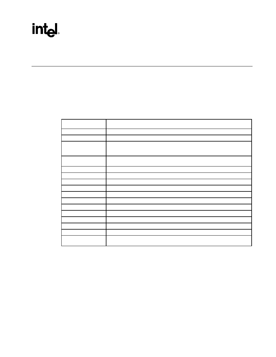
Table 5 lists the processor system signals by type. All AGTL signals are synchronous with the BCLK
and BCLK# signals. All TAP signals are synchronous with the TCK signal except TRST#. All CMOS
input signals can be applied asynchronously.
Table 5. System Signal Groups
Group Name
Signals
AGTL Input
BPRI#, DEFER#, RESET#, RSP#
AGTL Output
PRDY#
AGTL I/O
A[35:3]#, ADS#, AERR#, AP[1:0]#, BERR#, BINIT#, BNR#, BP[3:2]#, BPM[1:0]#,
BREQ0#, D[63:0]#, DBSY#, DEP[7:0]#, DRDY#, HIT#, HITM#, LOCK#, REQ[4:0]#, RP#,
RS[2:0]#, TRDY#
1.5 V CMOS Input
A20M#, DPSLP#, FLUSH#, IGNNE#, INIT#, LINT0/INTR, LINT1/NMI, PREQ#, SMI#,
STPCLK#
1.8 V CMOS Input
PWRGOOD
1.5 V Open Drain Output
FERR#, IERR#
3.3 V Open Drain Output
BSEL[1:0], VID[4:0]
1.25 V input
VTTPWRGD
Clock
BCLK, BCLK# (Differential Mode)
2.5 V Clock Input
BCLK (Single Ended Mode)
APIC Clock
PICCLK
APIC I/O
PICD[1:0]
Thermal Diode
THERMDC, THERMDA
TAP Input
TCK, TDI, TMS, TRST#
TAP Output
TDO
Power/Other
CLKREF, CMOSREF, EDGECTRLP, NC, NCTRL, PLL1, PLL2, RTTIMPEDP, VCC, VCCT,
VREF, VSS,
NOTES:
1. VCC is the power supply for the core logic.
2. PLL1 and PLL2 are power/ground for the PLL analog section. See Section 3.2.2 for details.
3. VCCT is the power supply for the system bus buffers.
4. VREF is the voltage reference for the AGTL input buffers.
5. VSS is system ground.
The APIC data and TAP outputs are Open-drain and should be pulled up to 1.5 V using resistors with the
values shown in Table 6. If Open-drain drivers are used for input signals, then they should also be pulled
up to the appropriate voltage using resistors with the values shown in Table 6.
相关PDF资料 |
PDF描述 |
|---|---|
| RJ80530VZ733256 | 32-BIT, 733 MHz, MICROPROCESSOR, PBGA479 |
| RH80530NZ001256 | 32-BIT, 1000 MHz, MICROPROCESSOR, CPGA478 |
| RJ80530VY700256 | 32-BIT, 700 MHz, MICROPROCESSOR, PBGA479 |
| RH80530WZ014256 | 32-BIT, 1333 MHz, MICROPROCESSOR, CPGA478 |
| RH80532NC021256 | 32-BIT, 1500 MHz, MICROPROCESSOR, CPGA478 |
相关代理商/技术参数 |
参数描述 |
|---|---|
| RH80530NZ009256 | 制造商:未知厂家 制造商全称:未知厂家 功能描述:MICROPROCESSOR|32-BIT|CMOS|PGA|478PIN|CERAMIC |
| RH80530NZ012256 | 制造商:Rochester Electronics LLC 功能描述:- Bulk |
| RH80530NZ014256 | 制造商:Rochester Electronics LLC 功能描述:- Bulk |
| RH80530WZ004256 | 制造商:Rochester Electronics LLC 功能描述:- Bulk |
| RH80530WZ006256 | 制造商:Rochester Electronics LLC 功能描述:- Bulk 制造商:Intel 功能描述: |
发布紧急采购,3分钟左右您将得到回复。