- 您现在的位置:买卖IC网 > PDF目录297329 > RT9205ACS (Richtek Technology Corporation) Dual Regulators - Synchronous Buck PWM DC-DC and Linear Controller PDF资料下载
参数资料
| 型号: | RT9205ACS |
| 厂商: | Richtek Technology Corporation |
| 英文描述: | Dual Regulators - Synchronous Buck PWM DC-DC and Linear Controller |
| 中文描述: | 双稳压器-同步降压PWM型DC - DC和线性控制器 |
| 文件页数: | 5/16页 |
| 文件大小: | 316K |
| 代理商: | RT9205ACS |
Preliminary
RT9205/A
DS9205/A-03 May 2003
www.richtek.com
13
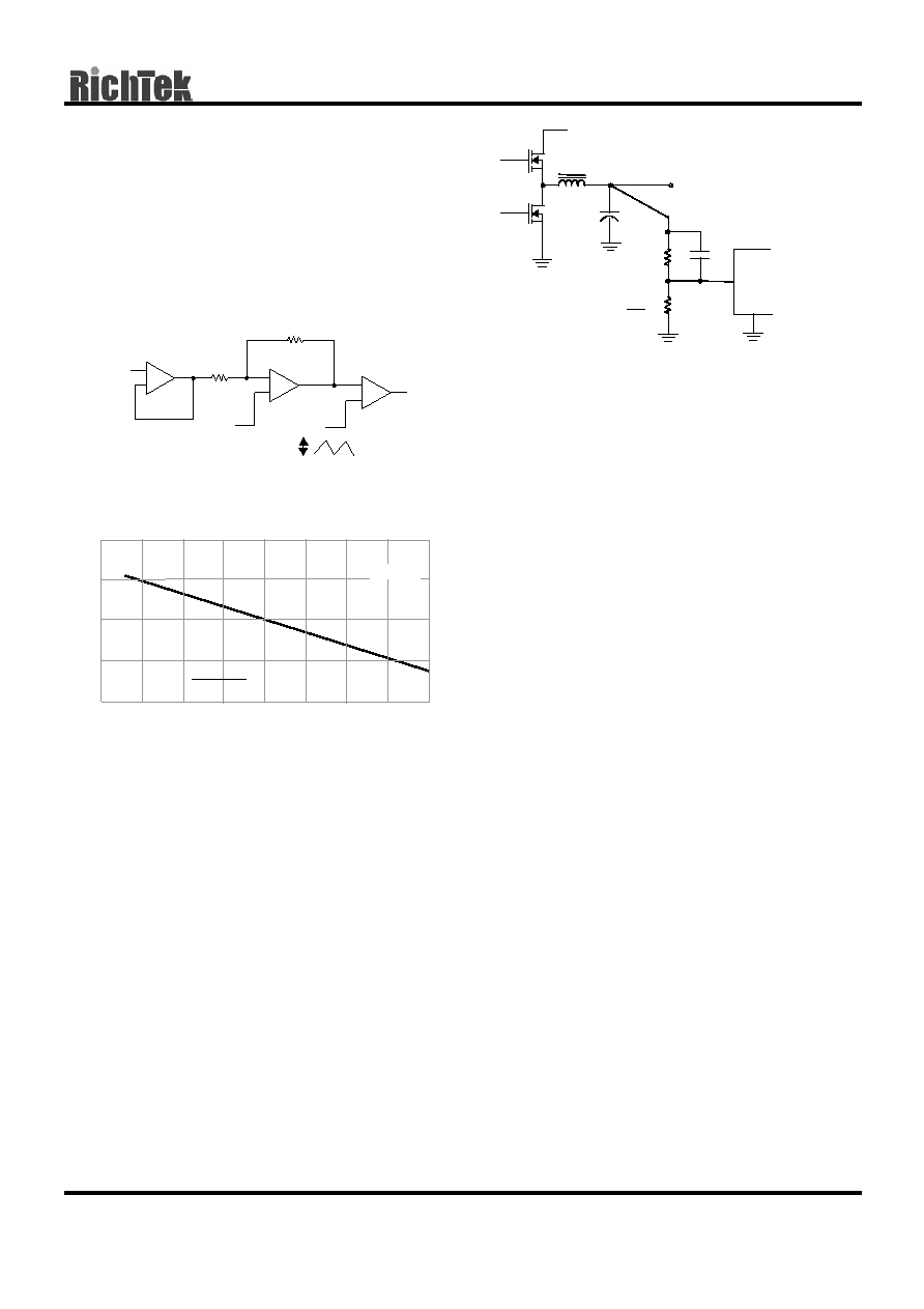
Reference Voltage
Because RT9205/A uses a low 35dB gain error
amplifier, as shown in Fig.10. The voltage regulation
is dependent on VIN and VOUT settings. The FB
reference voltage of 0.8V were trimmed at VIN = 5V
and VOUT = 2.5V. In a fixed VIN = 5V application, the
FB reference voltage vs. VOUT voltage can be
calculated as Fig.11.
Fig. 10
Fig. 11
Feedback Divider
The reference of RT9205/A is 0.8V. The output
voltage can be set using a resistor-divider as shown
in Fig.12. Put the R1 and R2 as close as possible to
FB pin. R2 value should be less than 1 k
to avoid
noise coupling issue. The C1 capacitor is a speed-up
capacitor for reducing output ripple to meet with the
requirement of fast transient load. Typically, value
between 1nF and 0.1
F is enough for C1.
Fig. 12
PWM Layout Considerations
MOSFETs switch very fast in efficiency. The speed
with which the current transitions from one device to
another
causes
voltage
spikes
across
the
interconnecting impedances and parasitic circuit
elements. The voltage spikes can degrade efficiency
and radiate noise, that results in over-voltage stress
on devices. Careful the layout for component
placement layout and printed circuit design can
minimize the voltage spikes induced in the converter.
Consider, as an example, the turn-off transition of the
upper MOSFET prior to turn-off, the upper MOSFET
was carrying the full load current. During turn-off,
current stops flowing in the upper MOSFET and is
picked up by the lower MOSFET or Schottky diode.
Any inductance in the switched current path
generates a large voltage spike during the switching
interval. Care with component selections, layout of
the critical components, and use shorter and wider
PCB traces that help in minimizing the magnitude of
voltage spikes.
There are two sets of critical components in a DC-DC
converter using the RT9205/A. The switching power
components are most critical because they switch
large amounts of energy, and as such, they tend to
generate equally large amounts of noise. The critical
small signal components are those connected to
sensitive nodes or those supplying critical bypass
current.
The power components and the PWM controller
should be placed firstly. Place the input capacitors,
especially the high-frequency ceramic decoupling
capacitors, close to the power switches. Place the
output inductor and output capacitors between the
+
_
+
_
EA
+
_
PWM
REP
0.8V
I3
56K
I2
1K
FB
RAMP
1.75V
FB
(
V
)
Duty (%)
VIN = 5V
80
70
60
20
30
40
50
0.82
0.78
0.80
0.81
0.79
10
90
VFB = 0.8V –
100
50
Duty
× 6.25mV
VOUT = VFB × (1+
2
1
R
)
VIN
COUT
+
VOUT
RT9205/A
FB
L
R1
R2
< 1K
C1
相关PDF资料 |
PDF描述 |
|---|---|
| RTB-1.5-2P | 2 CONTACT(S), MALE, STRAIGHT TWO PART BOARD CONNECTOR, SOLDER |
| RTB-1.5-3P | 3 CONTACT(S), MALE, STRAIGHT TWO PART BOARD CONNECTOR, SOLDER |
| RTB-1.5-4P | 4 CONTACT(S), MALE, STRAIGHT TWO PART BOARD CONNECTOR, SOLDER |
| RTB-1.5-5P | 5 CONTACT(S), MALE, STRAIGHT TWO PART BOARD CONNECTOR, SOLDER |
| RTB-1.5-6P | 6 CONTACT(S), MALE, STRAIGHT TWO PART BOARD CONNECTOR, SOLDER |
相关代理商/技术参数 |
参数描述 |
|---|---|
| RT9205-ACS | 制造商:RICHTEK 制造商全称:Richtek Technology Corporation 功能描述:Dual Regulators - Synchronous Buck PWM DC-DC and Linear Controller |
| RT9205AGS | 制造商:RICHTEK 制造商全称:Richtek Technology Corporation 功能描述:Dual Regulators - Synchronous Buck PWM DC-DC and Linear Controller |
| RT9205APS | 制造商:RICHTEK 制造商全称:Richtek Technology Corporation 功能描述:Dual Regulators - Synchronous Buck PWM DC-DC and Linear Controller |
| RT9205GS | 制造商:RICHTEK 制造商全称:Richtek Technology Corporation 功能描述:Dual Regulators - Synchronous Buck PWM DC-DC and Linear Controller |
| RT9205PS | 制造商:RICHTEK 制造商全称:Richtek Technology Corporation 功能描述:Dual Regulators - Synchronous Buck PWM DC-DC and Linear Controller |
发布紧急采购,3分钟左右您将得到回复。