- 您现在的位置:买卖IC网 > PDF目录69323 > RTC-4543SB:B-0 REAL TIME CLOCK, PDSO18 PDF资料下载
参数资料
| 型号: | RTC-4543SB:B-0 |
| 元件分类: | 时钟/数据恢复及定时提取 |
| 英文描述: | REAL TIME CLOCK, PDSO18 |
| 封装: | SOP-18 |
| 文件页数: | 2/16页 |
| 文件大小: | 224K |
RTC - 4543 SA/SB
Page
7
ETM09E-02
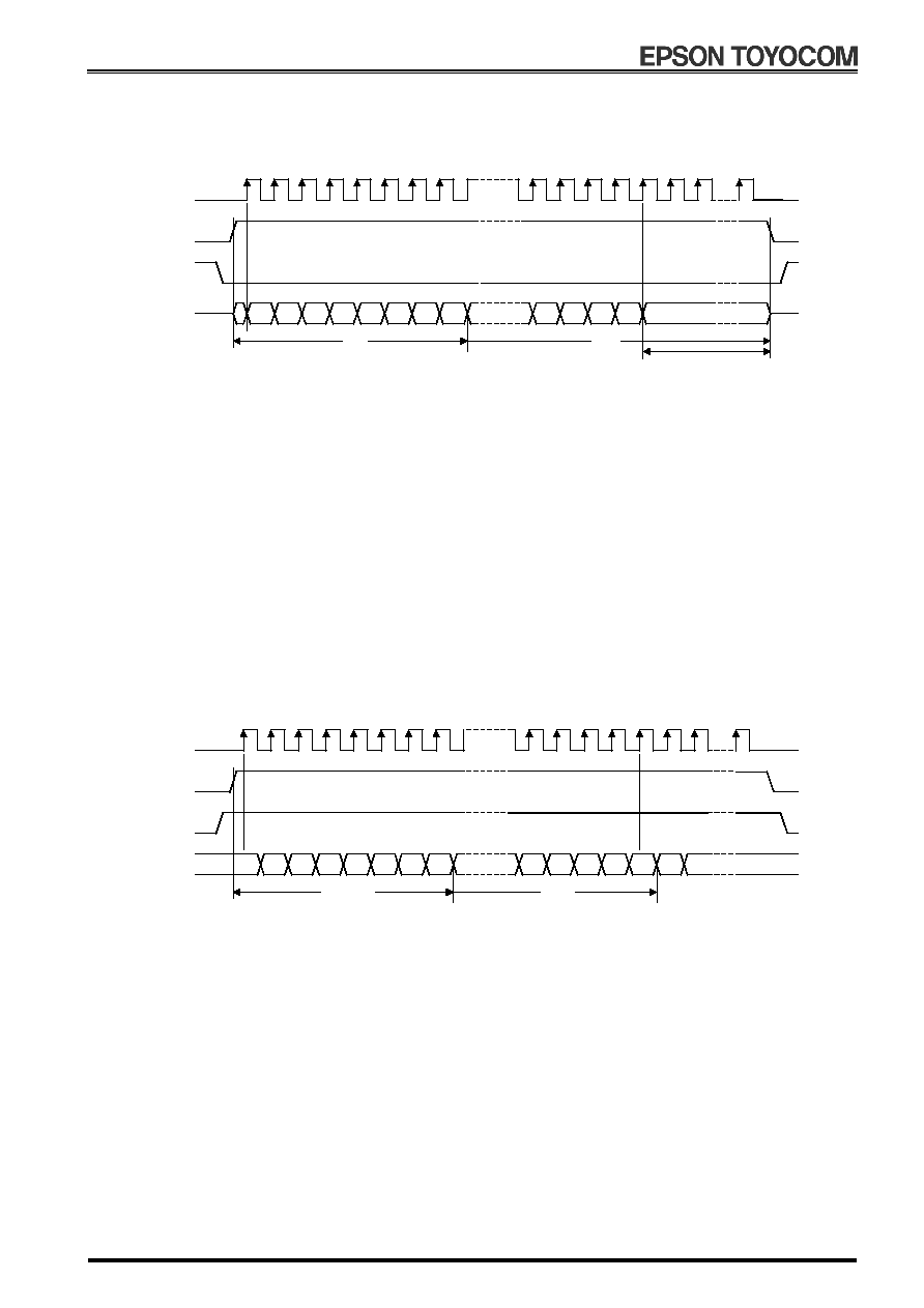
7. Description of Operation
7-1.Data reads
CLK
WR
DATA
FDT
s40
s20
s10
s8
s4
s2
s1
y8
y10 y20 y40
CE
y80
1
52
Sec
2
53
54
54+n
Output data does not change
Year
1)
When the WR pin is low and the CE pin is high, the RTC enters data output mode.
2)
At the first rising edge of the CLK signal, the clock and calendar data are loaded into the shift
register and the LSB of the seconds digits is output from the DATA pin.
3)
The remaining seconds, minutes, hour, day of the week, day, month, and year data is shifted out,
in sequence and in synchronization with the rising edge of the CLK signal, so that the data is
output from the DATA pin.
The output data is valid until the rising edge of the 52nd clock pulse; even if more than 52 clock
pulses are input, the output data does not change.
4)
If data is required in less than 52 clock pulses, that part of the data can be gotten by setting the
CE pin low after the necessary number of clock pulses have been output.
Example: If only the data from “seconds” to “day of the week” is needed:
After 28 clock pulses, set the CE pin low in order to get the data from “seconds” to “day of
the week.”
5)
When performing successive data read operations, a wait (tRCV) is necessary after the CE pin
is set low.
6)
Note that if an update operation (a one-second carry) occurs during a data read operation,
the data that is read will have an error of -1 second.
7)
Complete data read operations within tCE (Max.) = 0.9 seconds, as described earlier.
7-2. Data writes
CLK
WR
DATA
0
s40
s20
s10
s8
s4
s2
s1
y8
y10 y20 y40
CE
y80
1
52
( FDT )
2
53
54
54+n
Seconds
Year
1)
When the WR pin is high and the CE pin is high, the RTC enters data input mode.
2)
In this mode, data is input, in succession and in synchronization with the rising edge of the CLK
signal, to the shift register from the DATA pin, starting from the LSB of the seconds digits.
3)
The sub-seconds counter is reset between the falling edge of the first clock pulse and the rising
edge of the second clock pulse.
In addition, carries to the seconds counter are prohibited at the
falling edge of the first clock pulse.
4)
Note that during a data write operation, all 52 bits of data must be input.
When a CE terminal turned into low in a state of under 52 bits, data of a clock
and the data of calendar which excluded year and
bits do not change.
Therefore please verify the data of
bits and year if necessary.
If more than 52 bits of data are input, the 53rd and subsequent bits are ignored.
(The first 52 bits of data are valid.)
5)
After the last data is input to the shift register at the rising edge of the 52nd clock pulse, the
contents of the shift register are transferred to the timer counter.
6)
Once the CE pin is set low, the prohibition on carries to the seconds counter is lifted.
Complete data write operations within tCE (Max.) = 0.9 seconds, as described earlier.
7)
If a data read operation is to be performed immediately after a data write operation, a wait (tRCV)
is necessary after the CE pin is set low.
* Malfunction will result if illegal data is written.
Therefore, be certain to write legal data.
相关PDF资料 |
PDF描述 |
|---|---|
| RTC-4543SBB-3 | 0 TIMER(S), REAL TIME CLOCK, PDSO18 |
| RTC-4543SBB-0 | 0 TIMER(S), REAL TIME CLOCK, PDSO18 |
| RTC-4574NBB | 0 TIMER(S), REAL TIME CLOCK, PDSO22 |
| RTC-4574SAB-0 | 0 TIMER(S), REAL TIME CLOCK, PDSO14 |
| RTC-4574SAB-3 | 0 TIMER(S), REAL TIME CLOCK, PDSO14 |
相关代理商/技术参数 |
参数描述 |
|---|---|
| RTC4553 | 制造商:未知厂家 制造商全称:未知厂家 功能描述:SERIAL-INTERFACE REAL TIME CLOCK MODULE |
| RTC-4553 | 制造商:未知厂家 制造商全称:未知厂家 功能描述:SERIAL-INTERFACE REAL TIME CLOCK MODULE |
| RTC4553A | 制造商:未知厂家 制造商全称:未知厂家 功能描述:IC SMD |
| RTC-4553A | 制造商:未知厂家 制造商全称:未知厂家 功能描述:Real-Time Clock |
| RTC-4553A2 | 功能描述:IC REAL TIME CLOCK 14-SOIC RoHS:否 类别:集成电路 (IC) >> 时钟/计时 - 实时时钟 系列:- 产品培训模块:Obsolescence Mitigation Program 标准包装:1 系列:- 类型:时钟/日历 特点:警报器,闰年,SRAM 存储容量:- 时间格式:HH:MM:SS(12/24 小时) 数据格式:YY-MM-DD-dd 接口:SPI 电源电压:2 V ~ 5.5 V 电压 - 电源,电池:- 工作温度:-40°C ~ 85°C 安装类型:表面贴装 封装/外壳:8-WDFN 裸露焊盘 供应商设备封装:8-TDFN EP 包装:管件 |
发布紧急采购,3分钟左右您将得到回复。