- 您现在的位置:买卖IC网 > PDF目录297328 > RV5C348B (RICOH COMPANY LTD) 4-WIRE SERIAL INTERFACE PDF资料下载
参数资料
| 型号: | RV5C348B |
| 厂商: | RICOH COMPANY LTD |
| 元件分类: | XO, clock |
| 英文描述: | 4-WIRE SERIAL INTERFACE |
| 中文描述: | 0 TIMER(S), REAL TIME CLOCK, PDSO10 |
| 封装: | 4 X 2.90 MM, 1.20 MM HEIGHT, 0.50 MM PITCH, SSOP-10 |
| 文件页数: | 4/45页 |
| 文件大小: | 1276K |
| 代理商: | RV5C348B |
第1页第2页第3页当前第4页第5页第6页第7页第8页第9页第10页第11页第12页第13页第14页第15页第16页第17页第18页第19页第20页第21页第22页第23页第24页第25页第26页第27页第28页第29页第30页第31页第32页第33页第34页第35页第36页第37页第38页第39页第40页第41页第42页第43页第44页第45页
Rx5C348A/B
Register Settings
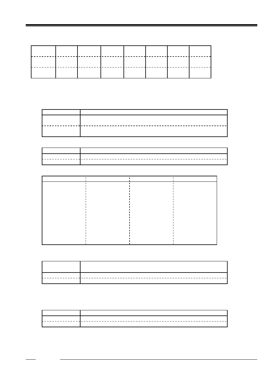
Control Register 1 (ADDRESS Eh)
D7
D6
D5
D4
D3
D2
D1
D0
WALE
DALE
/12
24
/CLEN2
*2)
TEST
CT2
CT1
CT0
(For Writing)
WALE
DALE
/12
24
/CLEN2
*2)
TEST
CT2
CT1
CT0
(For Reading)
0
Default
Settings
*1)
Default settings:
Default value means read / written values when the XSTP bit is set to “1” due to
VDD
power-on from 0v or oscillation stopping
*2)
This bit name applies to the Rx5C348A only.
For the Rx5C348B the bit name is SCRATCH3..
(1) WALE, DALEAlarm_W Enable Bit, Alarm_D Enable Bit
WALE,DALE
Description
0
Disabling the alarm interrupt circuit (under the control of the settings
of the Alarm_W registers and the Alarm_D registers).
(Default)
1
Enabling the alarm interrupt circuit (under the control of the settings
of the Alarm_W registers and the Alarm_D registers)
(2) /12
24
/12-24-hour Mode Selection Bit
/12
24
Description
0
Selecting the 12-hour mode with a.m. and p.m. indications.
(Default)
1
Selecting the 24-hour mode
Setting the /12
24 bit to 0 and 1 specifies the 12-hour mode and the 24-hour mode, respectively.
24-hour mode
12-hour mode
24-hour mode
12-hour mode
00
12 (AM12)
12
32 (PM12)
01
01 (AM 1)
13
21 (PM 1)
02
02 (AM 2)
14
22 (PM 2)
03
03 (AM 3)
15
23 (PM 3)
04
04 (AM 4)
16
24 (PM 4)
05
05 (AM 5)
17
25 (PM 5)
06
06 (AM 6)
18
26 (PM 6)
07
07 (AM 7)
19
27 (PM 7)
08
08 (AM 8)
20
28 (PM 8)
09
09 (AM 9)
21
29 (PM 9)
10
10 (AM10)
22
30 (PM10)
11
11 (AM11)
23
31 (PM11)
Setting the /12
24 bit should precede writing time data
(3) /CLEN2 (Rx5C348A)
32kHz Clock Output Bit 2
/CLEN2
Description
0
Enabling the 32-kHz clock circuit
(Default)
1
Disabling the 32-kHz clock circuit
Setting the /CLEN2 bit or the /CLEN1 bit (D3 in the control register 2) to 0, specifies generating clock pulses
with the oscillation frequency of the 32.768-kHz crystal oscillator for output from the 32KOUT pin.
Conversely, setting both the /CLEN1 and /CLEN2 bit to 1 disabling (”H”) such output.
SCRATCH3 (Rx5C348B)
Scratch Bit 3
SCRATCH3
Description
0
(Default)
1
For the Rx5C348B, this bit is intended for scratching and accepts the reading and writing of 0 and 1.
The
SCRATCH3 bit will be set to 0 when the XSTP bit is set to 1 in Control Register 2.
12345
Rev.2.01
- 12 -
相关PDF资料 |
PDF描述 |
|---|---|
| RS9EM18M | RECTANGULAR ADAPTER |
| TDH25FJ1212 | RECTANGULAR ADAPTER |
| TDH25FJ4545K | RECTANGULAR ADAPTER |
| TDH25MJ12D | RECTANGULAR ADAPTER |
| TDH25M00 | RECTANGULAR ADAPTER |
相关代理商/技术参数 |
参数描述 |
|---|---|
| RV5C386A | 制造商:RICOH 制造商全称:RICOH electronics devices division 功能描述:I2C-bus Real-Time Clock ICs with Voltage Monitoring Function |
| RV5C386A_03 | 制造商:RICOH 制造商全称:RICOH electronics devices division 功能描述:I2C bus SERIAL INTERFACE REAL-TIME CLOCK IC WITH VOLTAGE MONITORING FUNCTION |
| RV5C386A-E2 | 制造商:RICOH 制造商全称:RICOH electronics devices division 功能描述:I2C-bus Real-Time Clock ICs with Voltage Monitoring Function |
| RV5C387A | 制造商:RICOH 制造商全称:RICOH electronics devices division 功能描述:I2C-bus Real-Time Clock ICs with Voltage Monitoring Function |
| RV5C387A_03 | 制造商:RICOH 制造商全称:RICOH electronics devices division 功能描述:I2C bus SERIAL INTERFACE REAL-TIME CLOCK IC WITH VOLTAGE MONITORING FUNCTION |
发布紧急采购,3分钟左右您将得到回复。