- 您现在的位置:买卖IC网 > PDF目录219503 > S-817B22AY-BG 2.2 V FIXED POSITIVE LDO REGULATOR, 0.67 V DROPOUT, PBCY3 PDF资料下载
参数资料
| 型号: | S-817B22AY-BG |
| 元件分类: | 固定正电压单路输出LDO稳压器 |
| 英文描述: | 2.2 V FIXED POSITIVE LDO REGULATOR, 0.67 V DROPOUT, PBCY3 |
| 封装: | LEAD FREE, TO-92, 3 PIN |
| 文件页数: | 8/53页 |
| 文件大小: | 826K |
| 代理商: | S-817B22AY-BG |
第1页第2页第3页第4页第5页第6页第7页当前第8页第9页第10页第11页第12页第13页第14页第15页第16页第17页第18页第19页第20页第21页第22页第23页第24页第25页第26页第27页第28页第29页第30页第31页第32页第33页第34页第35页第36页第37页第38页第39页第40页第41页第42页第43页第44页第45页第46页第47页第48页第49页第50页第51页第52页第53页
SUPER-SMALL PACKAGE CMOS VOLTAGE REGULATOR
S-817 Series
Rev.5.0_00
Seiko Instruments Inc.
16
Selection of Output Capacitor (CL)
To stabilize operation against variation in output load, a capacitor (CL) must be mounted between VOUT
and VSS in the S-817 series because the phase is compensated with the help of the internal phase
compensation circuit and the ESR of the output capacitor.
When selecting a ceramic or an OS capacitor, capacitance should be 0.1
μF or more, and when selecting a
tantalum or an aluminum electrolytic capacitor, capacitance should be 0.1
μF or more and ESR 30 Ω or
less.
When an aluminum electrolytic capacitor is used attention should be especially paid to since the ESR of the
aluminum electrolytic capacitor increases at low temperature and possibility of oscillation becomes large.
Sufficient evaluation including temperature characteristics is indispensable.
Overshoot and undershoot
characteristics differ depending upon the type of the output capacitor.
Refer to CL dependencies in “
Reference Data 1. Transient Response Characteristics”.
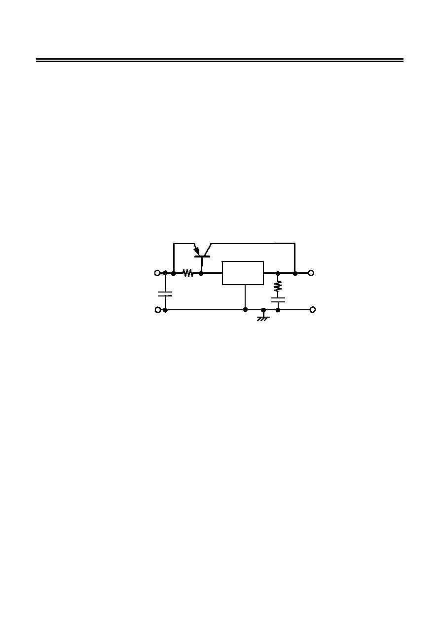
Application Circuits
1. Output Current Boosting Circuit
R2
R1
Tr1
GND
VOUT
VIN
VSS
VIN
VOUT
CL
S-817
series
CIN
Figure 15
As shown in Figure 15, the output current can be boosted by externally attaching a PNP transistor. The
base current of the PNP transistor is controlled so that output voltage (VOUT) goes the voltage specified
in the S-817 Series when base-emitter voltage (VBE) necessary to turn on the PNP transistor is obtained
between input voltage (VIN) and S-817 Series power source pin (VIN).
The following are tips and hints for selecting and ensuring optimum use of external parts
PNP transistor (Tr1):
1. Set hFE to approx. 100 to 400.
2. Confirm that no problem occurs due to power dissipation under normal operation conditions.
Resistor (R
1):
Generally set R1 to 1 kΩ ÷ VOUT (S) (the voltage specified in the S-817 Series) or more.
Output capacitor (C
L):
Output capacitor (CL) is effective in minimizing output fluctuation at powering on or due to power
or load fluctuation, but oscillation might occur. Always connect resistor R2 in series to output
capacitor CL.
Resistor (R
2): Set R2 to 2 Ω × VOUT(S) or more.
DO NOT attach a capacitor between the S-817 Series power source (V
IN) and GND pins or
between base and emitter of the PNP transistor to avoid oscillation.
To improve transient response characteristics of the output current boosting circuit shown in
Figure 15, check that no problem occurs due to output fluctuation at powering on or due to
power or load fluctuation under normal operating conditions.
Pay attention to the short current limit circuit incorporated into the S-817 Series because it does
not function as a shortcircuiting protection circuit for this boosting circuit.
相关PDF资料 |
PDF描述 |
|---|---|
| S-817B22AY-TG | 2.2 V FIXED POSITIVE LDO REGULATOR, 0.67 V DROPOUT, PBCY3 |
| S-817B22AY-ZG | 2.2 V FIXED POSITIVE LDO REGULATOR, 0.67 V DROPOUT, PBCY3 |
| S-817B31AMC-CWU-T2G | 3.1 V FIXED POSITIVE LDO REGULATOR, 0.41 V DROPOUT, PDSO5 |
| S-817B31AUA-CWU-T2G | 3.1 V FIXED POSITIVE LDO REGULATOR, 0.41 V DROPOUT, PSSO3 |
| S-817B31AY-BG | 3.1 V FIXED POSITIVE LDO REGULATOR, 0.41 V DROPOUT, PBCY3 |
相关代理商/技术参数 |
参数描述 |
|---|---|
| S-817B22AY-B-G | 制造商:Seiko Instruments Inc (SII) 功能描述:IC REG LDO 2.2V 35MA TO92-3 |
| S-817B22AY-X | 制造商:SII 制造商全称:Seiko Instruments Inc 功能描述:SUPER-SMALL PACKAGE CMOS VOLTAGE REGULATOR |
| S-817B22AY-X-G | 制造商:SII 制造商全称:Seiko Instruments Inc 功能描述:SUPER-SMALL PACKAGE CMOS VOLTAGE REGULATOR |
| S-817B23AMC-CWM-T2 | 制造商:SII 制造商全称:Seiko Instruments Inc 功能描述:SUPER-SMALL PACKAGE CMOS VOLTAGE REGULATOR |
| S-817B23AMC-CWMT2G | 功能描述:低压差稳压器 - LDO Linear LDO regulator 1.2uA Iq 75mA Iout RoHS:否 制造商:Texas Instruments 最大输入电压:36 V 输出电压:1.4 V to 20.5 V 回动电压(最大值):307 mV 输出电流:1 A 负载调节:0.3 % 输出端数量: 输出类型:Fixed 最大工作温度:+ 125 C 安装风格:SMD/SMT 封装 / 箱体:VQFN-20 |
发布紧急采购,3分钟左右您将得到回复。