- 您现在的位置:买卖IC网 > PDF目录96803 > S10064-01B LOGIC OUTPUT PHOTO DETECTOR PDF资料下载
参数资料
| 型号: | S10064-01B |
| 元件分类: | 光电元器件 |
| 英文描述: | LOGIC OUTPUT PHOTO DETECTOR |
| 封装: | PLASTIC PACKAGE-4 |
| 文件页数: | 1/2页 |
| 文件大小: | 249K |
| 代理商: | S10064-01B |
Features
Applications
PHOTO
IC
Transmitter/Receiver photo IC for optical link
For MOST automotive network, 50 Mbps band POF communications
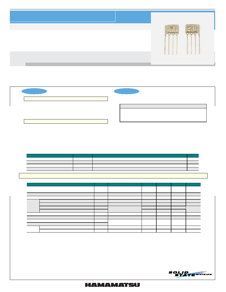
L10063-01, S10064-01B
L10063-01 and S10064-01B are transmitter and receiver photo ICs developed for MOST (Media Oriented System Transport) networks used in
vehicles to communicate multimedia information. The transmitter photo IC L10063-01 consists of a red LED and driver IC incorporated into a clear
plastic package and can be set to an operating mode that reduces the optical output level by half. The receiver photo IC S10064-01B is a monolithic
photo IC fabricated by the PiN-BiP process and features a wide dynamic range. It also has a low power consumption "sleeping mode" and an optical
wakeup mode triggered by input of light. Both the transmitter and receiver photo IC input or output digital signals through a TTL interface.
l Wide operating temperature range: -40 to +105 C
l DC to 50 Mbps data communications
l TTL input
l Optical output 50 % cut mode
l Only for vehicle networks (MOST)
L10063-01
S10064-01B
l Wide operating temperature range: -40 to +105 C
l 4 M to 50 Mbps data communications
l Monolithic structure immune from external noise
l TTL output
l Wide dynamic range
l Sleeping mode with optical wakeup
1
s A bsolu te m axim um ratings *
1 (Ta= -40 to +105
°C)
P a ram ete r
Sym b ol
L10063-01, S 1 0064-01B
Unit
S u pp ly vo ltag e
V cc
-0 .5 to + 7.0
V
O perating tem perature
To pr
-4 0 to + 105
°C
S torage tem p erature
Ts tg
-4 0 to + 120
°C
S o lderin g
Tso l
260 °C , 5 s, 3 tim es , at leas t 2.5 m m aw ay from le ad root
-
s E lectrica l a nd optical cha racteristics (Ta= -40 to +105
°C, Vcc=4.75 to 5.25 V *1)
Pa ra m e te r
Sym b o l
C o ndition
Min .
Typ .
Max.
Un it
C u rre n t co nsum ptio n
(o p e ra tio n m o d e )
Ic c o
*
2
-
3 0
m A
C u rre n t co nsum ptio n (s leep in g m ode )
Ic cs
Da rk s ta te
-
20
A
R e ce iver le ve l
P o pt3
B i-p hase sign a l
-2 5
-
-2
d B m
H ig h le ve l o u tp ut vo ltage
Voh
Ioh= -1 5 0 m
2.5
-
V cc+ 0.3
V
Lo w le ve l output vo ltag e
Vo l
Io l= 1.6 m A
0
-
0.4
V
R is e tim e
tr
-
9
Vout
Fall tim e
tf
10 to 90 % *
2, *3
-
7
ns
P u ls e w idth va ria tio n
tp w v
*
2, *3, *4, *6
17 .9
-
29 .7 9
ns
P u ls e w idth dis to rtion (a ve ra g e va lu e)
tapw d
*
2, *3, *4, *6
-2 .69
-
+ 6 .49
ns
Operation to sleeping mode transition receivable level
Ps l
Sleeping mode to operation transition receivable level
P op
*
2, *5
-3 9
-
-2 5 .5
d B m
H ig h le ve l vo ltage
V m h
Im h = -2 0 A
4 .0
-
V
Mo d e
ou tp ut
L o w le ve l vo lta ge
V m l
Im l= 0 .8 8 m A
-
0 .5
V
*1 : A bypa ss ca p acito r (0 .1 F ) is conn ecte d b e tw ee n V cc an d G N D at a p o sitio n w ith in 3 m m from th e lead , and a 10 F
c a p a c itor is a ls o c onne c ted to th e pow e r su pp ly line n e a rb y.
Th e ce nter of th e op tical fibe r is a lig ned w ith th e center o f the p a ckage len s .
T he dis ta n ce be tw e en the fiber e nd and th e le n s to p is 0.1 m m .
*2 : M e asu re d w ith in p u t sign als conform ing to S P 3 M O S T sp e c ific ation of p h ysical la ye r R e v 1.1 A d d end um B .
*3 : M e asu red w ith R L=5 0 k
, C L=15 pF (including parasitic capacitance such as probe, connector and evaluation circuit board
pa ttern ), and th re s h old vo ltage 1 .5 V.
*4 : A n o ptica l in put w a ve fo rm is g ene ra te d w ith a H a m a m a tsu stan da rd tran sm itte r.
*5 : A verag e optic al o u tp u t is m eas u red w ith a P O F (N A =0.5).
*6 : M e a s ured w ith B iP h ase P R B S at 45.2 M b p s (N R Z s ig n a l c onvers ion).
No te ) If m odu la te d light a t 4 M b p s o r le ss (inclu din g D C light a nd n o ligh t in pu t) is inpu t to S 1 0 0 64-0 1 B , th e high a nd lo w le ve ls
ca nno t be d iscern ed.
S10064-01B
MOST compliant products
Specifications of these products are subject to change
without prior notice to keep up with changes in the
MOST standard.
相关PDF资料 |
PDF描述 |
|---|---|
| S10109 | LOGIC OUTPUT PHOTO DETECTOR |
| S11MD4T | 1 CHANNEL TRIAC OUTPUT WITH ZERO CRSVR OPTOCOUPLER |
| S16-FREQ2-J-1-7-FT | QUARTZ CRYSTAL RESONATOR, 20 MHz - 25.999 MHz |
| S16-13.000MHZ-J-1-7-FR | QUARTZ CRYSTAL RESONATOR, 13 MHz |
| S16-16.000MHZ-J-1-7-FR | QUARTZ CRYSTAL RESONATOR, 16 MHz |
相关代理商/技术参数 |
参数描述 |
|---|---|
| S10065SP | 制造商:Pentair Technical Products / Hoffman 功能描述:FILTER, 1 BOX = QTY 4, 17X5 |
| S1006EWA | 功能描述:LED 显示器和配件 Orange RoHS:否 制造商:Avago Technologies 显示器类型:7 Segment 数位数量:2 字符大小:7.8 mm x 14.22 mm 照明颜色:Red 波长:628 nm 共用管脚:Common Anode 工作电压:2.05 V 工作电流:20 mA 最大工作温度:+ 85 C 最小工作温度:- 35 C 封装:Tube |
| S1006F1 | 制造商:TECCOR 制造商全称:TECCOR 功能描述:SCRs 1-70 AMPS NON-SENSITIVE GATE |
| S1006-KIT-1 | 功能描述:热收缩管和套管 RoHS:否 制造商:3M Electronic Specialty 类型:Tubing 材料:Polyolefin, Flexible 颜色:Clear 最低收缩温度:+ 100 C 恢复直径: 长度:100 ft 内径:1.5 in 收缩率:2:1 |
| S1006-KIT-8 | 制造商:TE Connectivity 功能描述:S1006-KIT-8 |
发布紧急采购,3分钟左右您将得到回复。