- 您现在的位置:买卖IC网 > PDF目录243484 > S1C88862F0A0100 MICROCONTROLLER, PQFP128 PDF资料下载
参数资料
| 型号: | S1C88862F0A0100 |
| 元件分类: | 微控制器/微处理器 |
| 英文描述: | MICROCONTROLLER, PQFP128 |
| 封装: | PLASTIC, QFP-128 |
| 文件页数: | 4/160页 |
| 文件大小: | 1244K |
| 代理商: | S1C88862F0A0100 |
第1页第2页第3页当前第4页第5页第6页第7页第8页第9页第10页第11页第12页第13页第14页第15页第16页第17页第18页第19页第20页第21页第22页第23页第24页第25页第26页第27页第28页第29页第30页第31页第32页第33页第34页第35页第36页第37页第38页第39页第40页第41页第42页第43页第44页第45页第46页第47页第48页第49页第50页第51页第52页第53页第54页第55页第56页第57页第58页第59页第60页第61页第62页第63页第64页第65页第66页第67页第68页第69页第70页第71页第72页第73页第74页第75页第76页第77页第78页第79页第80页第81页第82页第83页第84页第85页第86页第87页第88页第89页第90页第91页第92页第93页第94页第95页第96页第97页第98页第99页第100页第101页第102页第103页第104页第105页第106页第107页第108页第109页第110页第111页第112页第113页第114页第115页第116页第117页第118页第119页第120页第121页第122页第123页第124页第125页第126页第127页第128页第129页第130页第131页第132页第133页第134页第135页第136页第137页第138页第139页第140页第141页第142页第143页第144页第145页第146页第147页第148页第149页第150页第151页第152页第153页第154页第155页第156页第157页第158页第159页第160页
S1C88832/88862 TECHNICAL MANUAL
EPSON
93
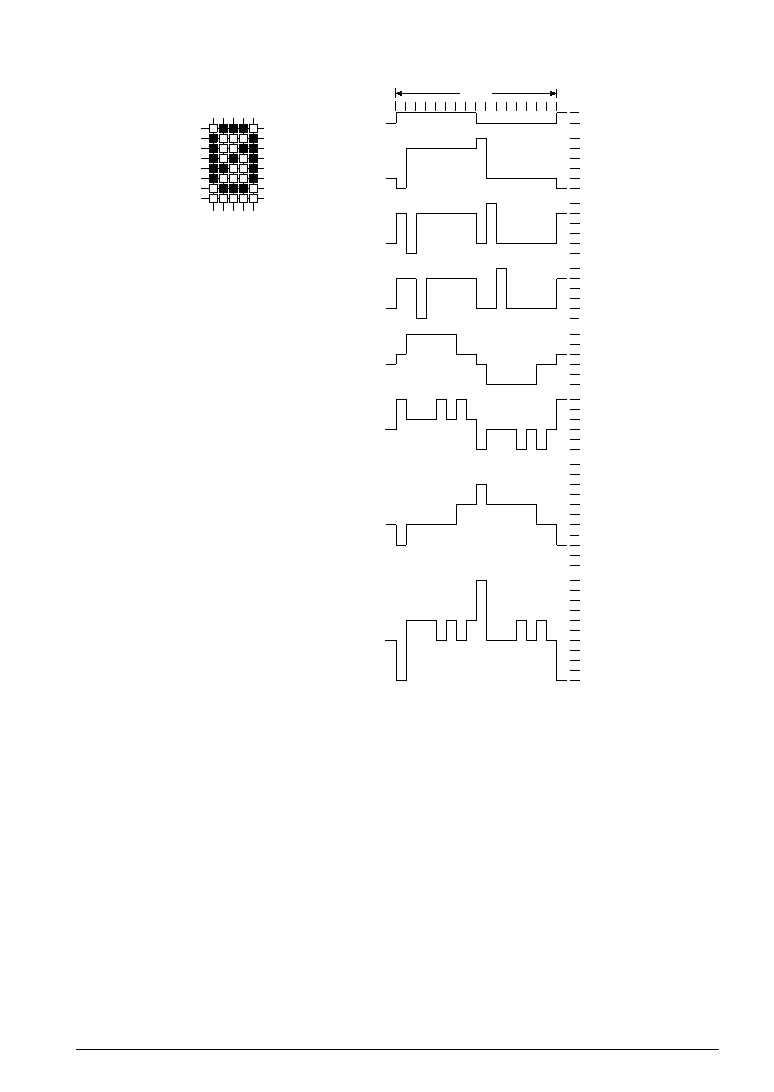
5 PERIPHERAL CIRCUITS AND THEIR OPERATION (LCD Controller)
Fig. 5.11.4.3
Drive waveform for 1/8 duty
5.11.5 Display memory
The S1C88832 has a built-in 402-byte display
memory. The S1C88862 has a built-in 342-byte
display memory. The display memory is allocated
to address F800H–FD42H (including unavailable
areas) and the correspondence between the
memory bits and common/segment terminal is
changed according to the selection status of the
following items.
(1) Drive duty (1/32, 1/16 or 1/8 duty)
(2) Dot font (5
× 8 or 5 × 5 dots)
When 1/16 or 1/8 duty is selected for drive duty,
two-screen memory can be secured, and the two
screens can be switched by the display memory
area selection register DSPAR. When "0" is written
to DSPAR, display area 0 is selected and when "1" is
written, display area 1 is selected.
Furthermore, memory allocation for 5
× 8 dots and
5
× 5 dots can be selected in order to easily display
5
× 5-dot font characters on the LCD panel.
This selection can be done by the dot font selection
register DTFNT: when "0" is written to DTFNT, 5
×
8 dots is selected and when "1" is written, 5
× 5 dots
is selected.
The correspondence between the display memory
bits set according to the drive duty and font size,
and the common/segment terminals are shown in
Figures 5.11.5.1–5.11.5.6.
When "1" is written to the display memory bit
corresponding to the dot on the LCD panel, the dot
goes ON and when "0" is written, it goes OFF. Since
display memory is designed to permit reading/
writing, it can be controlled in bit units by logical
operation instructions and other means (read,
modify and write instruction)s.
The display memory bits that have not been
assigned can be used as general purpose RAM with
read/write capabilities. Even when external
memory has expanded into the display memory
area, this area is not released to external memory.
Access to this area is always via display memory.
COM0
1
2
3
4
5
6
7
SEG0
1
2
3
4
VDD
VSS
VC5
VC4
VC3
VC2
VC1
VSS
7
3
2
1
0
7
3
2
1
0
FR
COM0
COM1
COM2
SEG0
SEG1
VC5
VC4
VC3
VC2
VC1
VSS
VC5
VC4
VC3
VC2
VC1
VSS
VC5
VC4
VC3
VC2
VC1
VSS
VC5
VC4
VC3
VC2
VC1
VSS
VC5
VC4
VC3
VC2
VC1
VSS (GND)
VC5
VC4
VC3
VC2
VC1
VSS (GND)
COM0–SEG0
COM0–SEG1
4
6
4
6
55
-VC1
-VC2
-VC3
-VC4
-VC5
-VC1
-VC2
-VC3
-VC4
-VC5
64 Hz
相关PDF资料 |
PDF描述 |
|---|---|
| STM8AF6146TDXXXX | MICROCONTROLLER, PQFP32 |
| STM32F105RBT7XXX | 32-BIT, FLASH, 72 MHz, RISC MICROCONTROLLER, PQFP64 |
| ST72F63BK6B1 | 8-BIT, FLASH, 8 MHz, MICROCONTROLLER, PDIP32 |
| ST72P63BE6M1 | 8-BIT, MROM, 8 MHz, MICROCONTROLLER, PDSO24 |
| SC104002MPV | 16-BIT, FLASH, 40 MHz, MICROCONTROLLER, PQFP112 |
相关代理商/技术参数 |
参数描述 |
|---|---|
| S1C8F360D411000 | 功能描述:16位微控制器 - MCU 8-bit Flash 60KB LCD Dr. 51 x 32 RoHS:否 制造商:Texas Instruments 核心:RISC 处理器系列:MSP430FR572x 数据总线宽度:16 bit 最大时钟频率:24 MHz 程序存储器大小:8 KB 数据 RAM 大小:1 KB 片上 ADC:Yes 工作电源电压:2 V to 3.6 V 工作温度范围:- 40 C to + 85 C 封装 / 箱体:VQFN-40 安装风格:SMD/SMT |
| S1C8F360D511000 | 功能描述:16位微控制器 - MCU 8-bit Flash 60KB LCD Dr. 51 x 32 RoHS:否 制造商:Texas Instruments 核心:RISC 处理器系列:MSP430FR572x 数据总线宽度:16 bit 最大时钟频率:24 MHz 程序存储器大小:8 KB 数据 RAM 大小:1 KB 片上 ADC:Yes 工作电源电压:2 V to 3.6 V 工作温度范围:- 40 C to + 85 C 封装 / 箱体:VQFN-40 安装风格:SMD/SMT |
| S1C8F360F413100 | 功能描述:16位微控制器 - MCU 8-bit Flash 60KB LCD Dr. 51 x 32 RoHS:否 制造商:Texas Instruments 核心:RISC 处理器系列:MSP430FR572x 数据总线宽度:16 bit 最大时钟频率:24 MHz 程序存储器大小:8 KB 数据 RAM 大小:1 KB 片上 ADC:Yes 工作电源电压:2 V to 3.6 V 工作温度范围:- 40 C to + 85 C 封装 / 箱体:VQFN-40 安装风格:SMD/SMT |
| S1C8F360F513200 | 功能描述:16位微控制器 - MCU 8-bit Flash 60KB LCD Dr. 51 x 32 RoHS:否 制造商:Texas Instruments 核心:RISC 处理器系列:MSP430FR572x 数据总线宽度:16 bit 最大时钟频率:24 MHz 程序存储器大小:8 KB 数据 RAM 大小:1 KB 片上 ADC:Yes 工作电源电压:2 V to 3.6 V 工作温度范围:- 40 C to + 85 C 封装 / 箱体:VQFN-40 安装风格:SMD/SMT |
| S1C8F626 | 制造商:EPSON 制造商全称:EPSON 功能描述:8-bit Single Chip Microcomputer |
发布紧急采购,3分钟左右您将得到回复。