- 您现在的位置:买卖IC网 > PDF目录98069 > S2024B-8 (APPLIEDMICRO INC) 32-BIT, DSP-CROSSBAR SWITCH, PQFP196 PDF资料下载
参数资料
| 型号: | S2024B-8 |
| 厂商: | APPLIEDMICRO INC |
| 元件分类: | 数字信号处理外设 |
| 英文描述: | 32-BIT, DSP-CROSSBAR SWITCH, PQFP196 |
| 封装: | HEAT SINK, NON CONDUCTIVE TIE-BAR, LDCC-196 |
| 文件页数: | 8/15页 |
| 文件大小: | 114K |
| 代理商: | S2024B-8 |
2
S2024
“CROSSBOW” 32 X 32 800 MBIT/S CROSSPOINT SWITCH
June 15, 1999 / Revision B
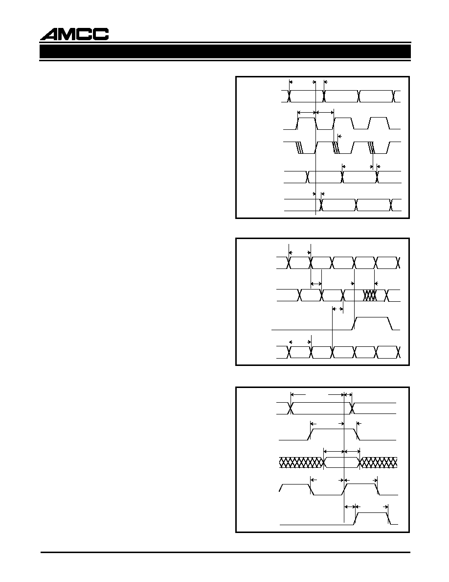
OPERATING MODES
SYNCHRONOUS MODE
In synchronous mode, two clock signals, MDCLK for
data input and SDCLK for data output, provide the latch
enable strobes to allow the input data and output data
to be stored in 32-bit latches. The S2024 is capable of
400-Mbit/s operation in this mode. The data is latched
on the falling edge of SDCLK and MDCLK.
Inputs MDCLK/MDCLKN and SDCLK/SDCLKN can be
used as true differentials or as single-ended clocking
signals. Onboard voltage reference outputs VBB1 and
VBB2 allow single-ended clocking capability when con-
figured as shown in Figure 8.
TRANSPARENT MODE
In transparent, or asynchronous, mode, any data ap-
pearing at the input will be passed immediately through
to its designated output. Transparent transfer of data
through the latches takes place when both MDCLK and
SDCLK clock inputs are held high. In this mode the
S2024 is capable of up to a 800 Mbit/s NRZ data rate.
RECONFIGURATION MODE
The S2024 can be selectively reconfigured one output
at a time, or any number of outputs can be reconfigured
simultaneously.Configurationdataisstoredin32registers,
one register for each output data pin. The 6-bit content
of each register selects the input data pin which is to be
connected to that output data pin. To connect an output
to a given input, the output to reconfigure is selected
using OUTADD0–4 and OAEN to enable the appropriate
output configuration register. With the output configura-
tion register selected, the desired input pin connection
is provided on INADD0–5. The input pin selection on
INADD0–5 will be stored into the selected output con-
figuration register on the rising edge of CNFGCLK.
When the switch is to be reconfigured, the S2024 mini-
mizes the time required through the use of an additional
configuration latch. While the switch is operational (and
prior to the time at which it must be reconfigured) a new
set of input addresses can be loaded into the register
file. When all registers have been updated, the contents
of the registers are parallel-transferred to the configura-
tion latch, when CNFGSTB goes high. This process
allows a switch reconfiguration in just 4 ns.
Figure 2. Synchronous Mode
DIN–31
MDCLK/N
SDCLK/N
XDIN–31
DOUT–31
t
SUDI
tHDI
A
B
C
A
B
A
B
MC
MPWH
MC
MPWL
t OVRL
t SUXDI
t HXDI
t SCKDO
Figure 3. Transparent Mode
CNFGSTB
A
B
C
D
E
A
B
CD
E
DOUT–31
DIN–31
tDIDO
tCFDO
A
B
C
D
E
XIN–31
DIMPW
tXIDO
XI MPW
Figure 4. Reconfiguration Mode
OUTADD–4
OAEN
SUOA
t
t HOA
ADDRESS VALID
t
SUOAE
t HOAE
CC
INADD–5
CNFGCLK
CNFGSTB
VALID
MPWL
MPWH
SUCFC
t
CSMPWH
SUIA
tt HIA
相关PDF资料 |
PDF描述 |
|---|---|
| S2025A | 32-BIT, DSP-CROSSBAR SWITCH, PQFP196 |
| S2025C-15 | 32-BIT, DSP-CROSSBAR SWITCH, PQFP196 |
| S2028A | 32-BIT, DSP-CROSSBAR SWITCH, PQFP224 |
| S202S15V | TRIGGER OUTPUT SOLID STATE RELAY, 3000 V ISOLATION-MAX |
| S202S15F | TRIGGER OUTPUT SOLID STATE RELAY, 3000 V ISOLATION-MAX |
相关代理商/技术参数 |
参数描述 |
|---|---|
| S2025L | 功能描述:SCR 25A 200V RoHS:否 制造商:STMicroelectronics 最大转折电流 IBO:480 A 额定重复关闭状态电压 VDRM:600 V 关闭状态漏泄电流(在 VDRM IDRM 下):5 uA 开启状态 RMS 电流 (It RMS): 正向电压下降:1.6 V 栅触发电压 (Vgt):1.3 V 最大栅极峰值反向电压:5 V 栅触发电流 (Igt):35 mA 保持电流(Ih 最大值):75 mA 安装风格:Through Hole 封装 / 箱体:TO-220 封装:Tube |
| S-2025L | 制造商:LITTELFUSE 制造商全称:Littelfuse 功能描述:RoHS Compliant, Electrically-isolated package |
| S2025L | 制造商:Littelfuse 功能描述:SCR Thyristor |
| S2025L | 制造商:Littelfuse 功能描述:THYRISTOR 200V 25A TO-220IS |
| S2025L_ | 功能描述:SCR USE 576-S2025L RoHS:否 制造商:STMicroelectronics 最大转折电流 IBO:480 A 额定重复关闭状态电压 VDRM:600 V 关闭状态漏泄电流(在 VDRM IDRM 下):5 uA 开启状态 RMS 电流 (It RMS): 正向电压下降:1.6 V 栅触发电压 (Vgt):1.3 V 最大栅极峰值反向电压:5 V 栅触发电流 (Igt):35 mA 保持电流(Ih 最大值):75 mA 安装风格:Through Hole 封装 / 箱体:TO-220 封装:Tube |
发布紧急采购,3分钟左右您将得到回复。