- 您现在的位置:买卖IC网 > PDF目录98069 > S2028A (APPLIEDMICRO INC) 32-BIT, DSP-CROSSBAR SWITCH, PQFP224 PDF资料下载
参数资料
| 型号: | S2028A |
| 厂商: | APPLIEDMICRO INC |
| 元件分类: | 数字信号处理外设 |
| 英文描述: | 32-BIT, DSP-CROSSBAR SWITCH, PQFP224 |
| 封装: | LDCC-224 |
| 文件页数: | 12/20页 |
| 文件大小: | 147K |
| 代理商: | S2028A |
2
33 x 32 1.25 GBIT/S DIFFERENTIAL CROSSPOINT SWITCH
S2028
July 2, 1999 / Revision C
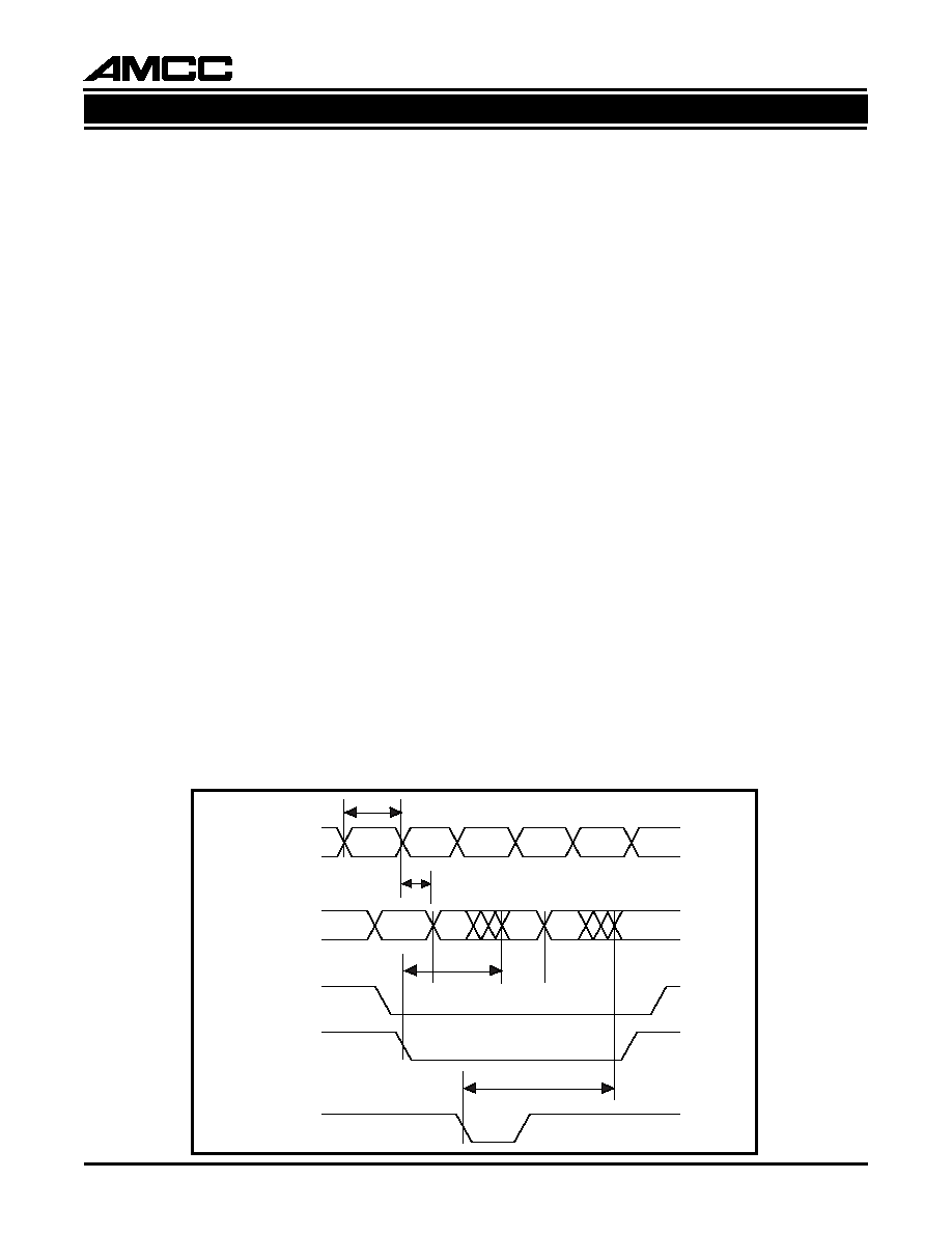
Figure 2. Data Transfer Waveforms
tCFDO
tLDDO
tDIDO
DIMPW
DIN [31:0] P/N
ADVERTISEP/N
DOUT [31:0] P/N
CONFIGN
LOADN
A
AB
C
D
E
BC
DE
CSN
Data Transfer
For each configured connection between a differen-
tial input pair and an enabled output pair, any data
appearing at the input pair and switching at up to
1.25 Gb/s will be passed immediately through to the
output pair.
Configuration
The S2028 can be selectively reconfigured one out-
put channel at a time in unicast mode, 16 output
channels at a time in multicast mode, and all 32
output channels simultaneously in broadcast mode.
Any number of output channels can be reconfigured
simultaneously using the CONFIGN control. Con-
figuration data is stored in all 32 registers, one
register for each output channel. As shown in Figure
1, the configuration data is passed in parallel from
all 32 registers to a bank of latches which hold the
active switch configuration. This two-state arrange-
ment allows any number of output channels to be
reconfigured simultaneously.
Each output configuration register holds 6 bits. Five
bits are used to select which input channel will be
connected to the output channel, and one bit is used
to override the input address and instead channel
the ADVERTISEP/N input to that output.
The S2028A 33 X 32 Crosspoint Switch interface is
designed to connect directly to a microprocessor’s
address and data bus and R/W signal. A CS input
(CSN) is provided to simplify interfacing to the
microprocessor’s address bus. Most of the device’s
functions can be programmed by a single instruction
in firmware. See the memory map in Figure 3. The
memory map depends on the hardware interface,
and can be mapped to any 1024 byte address range.
In general, the address bus will specify the
crosspoint switch input channel, and the data bus
will specify the crosspoint switch output channel.
The microprocessor or host hardware presents the
address and data to the S2028A, the decoder logic
enables CSN, and then the microprocessor strobes
the Read/Write* signal (LOADN). (See Figure 2.)
Broadcast Mode
Writing to any address in the Broadcast Address
Space (512-1023) will broadcast the input channel
specified on the address bus (IADDR) to all 32 out-
put channels. If the ADVERT bit is set to a 1, IADDR
is ignored and the ADVERTISE input is broadcast to
all 32 output channels. Broadcasting is a single cycle
operation, and does not require strobing of
CONFIGN.
TTL configuration controls simplify interfacing to
slower speed circuitry. Once a new configuration
has been entered into the configuration register file,
the S2028 can be completely reconfigured in only
10 ns without disturbing switch operations.
The configuration register can also be put into trans-
parent mode, reconfiguring all addressed outputs
within 10ns after the LOADN signal goes low.
相关PDF资料 |
PDF描述 |
|---|---|
| S202S15V | TRIGGER OUTPUT SOLID STATE RELAY, 3000 V ISOLATION-MAX |
| S202S15F | TRIGGER OUTPUT SOLID STATE RELAY, 3000 V ISOLATION-MAX |
| S202SE2 | TRIGGER OUTPUT SOLID STATE RELAY, 3000 V ISOLATION-MAX |
| S3C1850XX-SM | 4-BIT, MROM, 6 MHz, MICROCONTROLLER, PDSO24 |
| S3C3410XXX-QA | 32-BIT, MROM, 40 MHz, RISC MICROCONTROLLER, PQFP128 |
相关代理商/技术参数 |
参数描述 |
|---|---|
| S2029-09-34 | 制造商:MISC. CONNECTORS 功能描述: |
| S202B | 制造商:Cinch Connectors 功能描述:CONN SOCKET2POS SOLDER 制造商:Cinch Connectors 功能描述:S202B/REY SPECIAL |
| S-202-B | 功能描述:Jones 插头和插槽 2P JONES SOCKET SLDR CABLE MNT RoHS:否 制造商:Molex 产品类型:Socket Connectors 系列:Beau 位置/触点数量:8 电压额定值:250 V 电流额定值:10 A 外壳材料:Thermoplastic 触点材料:Phosphor Bronze 触点电镀:Tin-Lead |
| S202-B20 | 制造商:ABB Low Voltage Products and Systems 功能描述:Minature Circuit Breaker, 2 Pole, B Trip, 20A, 400 VAC |
| S202-B25 | 制造商:ABB Control 功能描述:MCB 2P B 25A 480Y/277 SUPP |
发布紧急采购,3分钟左右您将得到回复。