- 您现在的位置:买卖IC网 > PDF目录225140 > S29CD016G0MFAN003 (SPANSION LLC) 16 Megabit (512 K x 32-Bit) CMOS 2.5 Volt-only Burst Mode, Dual Boot, Simultaneous Read/Write Flash Memory PDF资料下载
参数资料
| 型号: | S29CD016G0MFAN003 |
| 厂商: | SPANSION LLC |
| 元件分类: | PROM |
| 英文描述: | 16 Megabit (512 K x 32-Bit) CMOS 2.5 Volt-only Burst Mode, Dual Boot, Simultaneous Read/Write Flash Memory |
| 中文描述: | 512K X 32 FLASH 2.7V PROM, 64 ns, PBGA80 |
| 封装: | 13 X 11 MM, 1 MM PITCH, FORTIFIED, BGA-80 |
| 文件页数: | 17/81页 |
| 文件大小: | 1276K |
| 代理商: | S29CD016G0MFAN003 |
第1页第2页第3页第4页第5页第6页第7页第8页第9页第10页第11页第12页第13页第14页第15页第16页当前第17页第18页第19页第20页第21页第22页第23页第24页第25页第26页第27页第28页第29页第30页第31页第32页第33页第34页第35页第36页第37页第38页第39页第40页第41页第42页第43页第44页第45页第46页第47页第48页第49页第50页第51页第52页第53页第54页第55页第56页第57页第58页第59页第60页第61页第62页第63页第64页第65页第66页第67页第68页第69页第70页第71页第72页第73页第74页第75页第76页第77页第78页第79页第80页第81页
22
S29CD-G Flash Family
S29CD-G_00_B1 March 3, 2009
Data
Sheet
(Pre limin ar y)
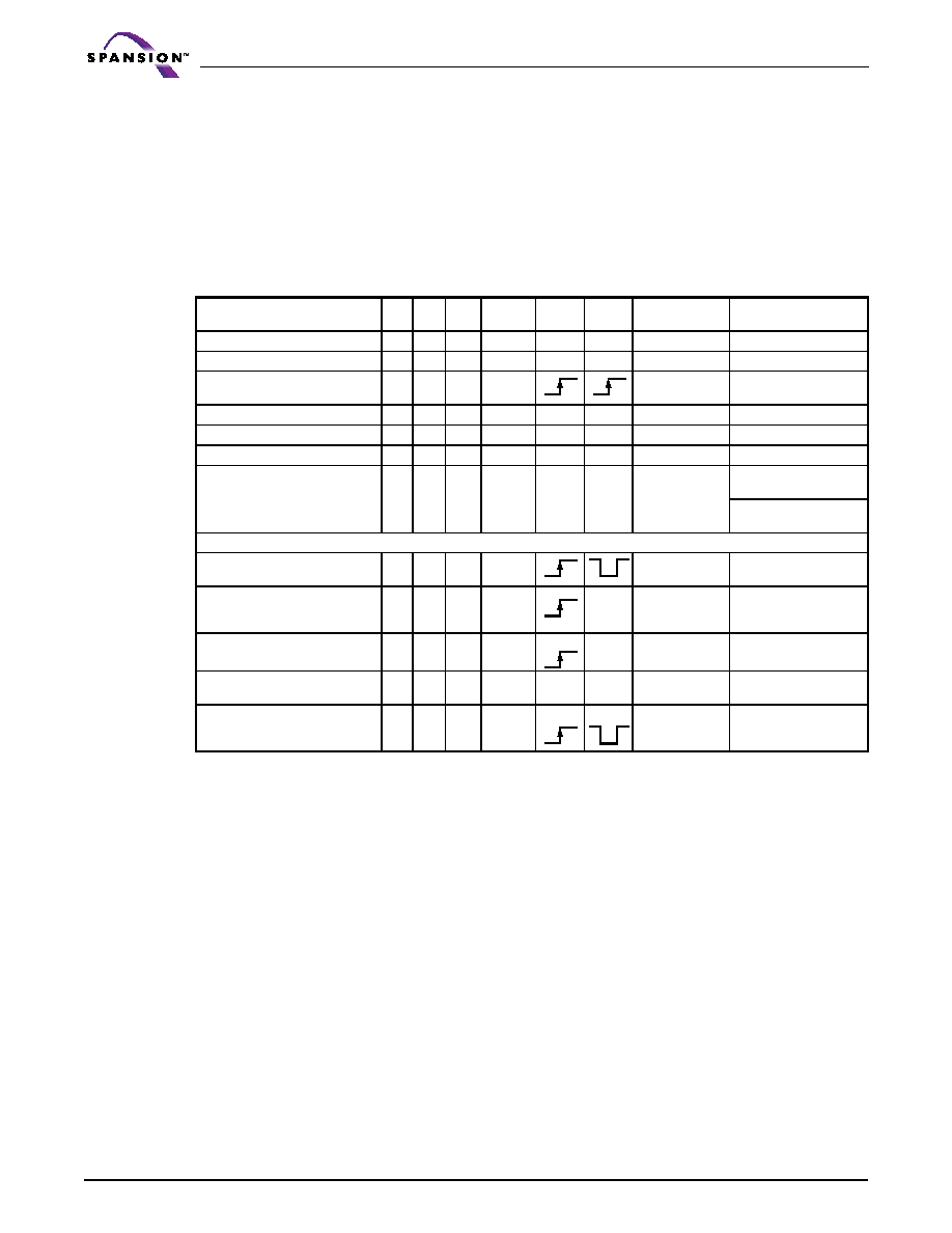
12. Device Operations
This section describes the requirements and use of the device bus operations, which are initiated through the
internal command register. The command register itself does not occupy any addressable memory location.
The register is composed of latches that store the commands, along with the address and data information
needed to execute the command. The contents of the register serve as inputs to the internal state machine.
The state machine outputs dictate the function of the device. Table 12.1 lists the device bus operations, the
inputs and control levels they require, and the resulting output. The following subsections describe each of
these operations in further detail.
Legend
L = Logic Low = VIL
H = Logic High = VIH
X = Don’t care.
Notes
1. WP# controls the two outermost sectors of the top boot block or the two outermost sectors of the bottom boot block.
2. DQ0 reflects the sector PPB (or sector group PPB) and DQ1 reflects the DYB
12.1
VersatileI/O (VIO) Control
The VersatileI/O (VIO) control allows the host system to set the voltage levels that the device generates at its
data outputs and the voltages tolerated at its data inputs to the same voltage level that is asserted on the VIO
pin.
The output voltage generated on the device is determined based on the VIO (VCCQ) level. For the 2.6 V VCC
Mask Option, a VIO of 1.65 V – 1.95 V allows the device to interface with I/Os lower than 2.5 V. Vcc = VIO (2.5
V to 2.75V) make the device appear as a 2.5 V only.
Table 12.1 Device Bus Operation
Operation
CE#
OE#
WE#
RESET#
CLK
ADV#
Addresses
Data
(DQ0–DQ31)
Read
L
H
X
AIN
DOUT
Asynchronous Write
L
H
L
H
X
AIN
DIN
Synchronous Write
L
H
L
H
AIN
DIN
Standby (CE#)
H
X
H
X
HIGH Z
Output Disable
L
H
X
HIGH Z
Reset
X
L
X
HIGH Z
PPB Protection Status (Note 2)
L
H
X
Sector Address,
A9 = VID,
A7 – A0 = 02h
00000001h, (protected)
A6 = H
00000000h (unprotect)
A6 = L
Burst Read Operations
Load Starting Burst Address
L
X
H
AIN
X
Advance Burst to next address
with appropriate Data presented
on the Data bus
L
H
X
Burst Data Out
Terminate Current Burst
Read Cycle
H
X
H
X
HIGH Z
Terminate Current Burst
Read Cycle with RESET#
XX
H
L
X
HIGH Z
Terminate Current Burst
Read Cycle;
Start New Burst Read Cycle
LH
H
AIN
X
相关PDF资料 |
PDF描述 |
|---|---|
| S29CD016G0MFAN010 | 16 Megabit (512 K x 32-Bit) CMOS 2.5 Volt-only Burst Mode, Dual Boot, Simultaneous Read/Write Flash Memory |
| S29CD032G0JFFN002 | 1M X 32 FLASH 2.7V PROM, 67 ns, PBGA80 |
| S29CD032G0RFFN003 | 1M X 32 FLASH 2.7V PROM, 48 ns, PBGA80 |
| S29CD032G0RQFI012 | 1M X 32 FLASH 2.7V PROM, 48 ns, PQFP80 |
| S29CL032J0JFAM020 | 1M X 32 FLASH 3.3V PROM, 54 ns, PBGA80 |
相关代理商/技术参数 |
参数描述 |
|---|---|
| S29CD016G0MFAN010 | 制造商:SPANSION 制造商全称:SPANSION 功能描述:16 Megabit (512 K x 32-Bit) CMOS 2.5 Volt-only Burst Mode, Dual Boot, Simultaneous Read/Write Flash Memory |
| S29CD016G0MFAN011 | 制造商:SPANSION 制造商全称:SPANSION 功能描述:16 Megabit (512 K x 32-Bit) CMOS 2.5 Volt-only Burst Mode, Dual Boot, Simultaneous Read/Write Flash Memory |
| S29CD016G0MFAN012 | 制造商:SPANSION 制造商全称:SPANSION 功能描述:16 Megabit (512 K x 32-Bit) CMOS 2.5 Volt-only Burst Mode, Dual Boot, Simultaneous Read/Write Flash Memory |
| S29CD016G0MFAN013 | 制造商:SPANSION 制造商全称:SPANSION 功能描述:16 Megabit (512 K x 32-Bit) CMOS 2.5 Volt-only Burst Mode, Dual Boot, Simultaneous Read/Write Flash Memory |
| S29CD016G0MFFA000 | 制造商:SPANSION 制造商全称:SPANSION 功能描述:32 Megabit (1M x 32-Bit), 16 Megabit (512K x 32-Bit) 2.5 Volt-only Burst Mode, Dual Boot, Simultaneous Read/ Write Flash Memory with VersatileI/O |
发布紧急采购,3分钟左右您将得到回复。